
Kang Liu, Hua-Rui Sun. Raman thermometry based thermal resistance analysis of GaN high electron mobility transistors with copper-based composite flanges [J]. Acta Physica Sinica, 2020, 69(2): 028501-1
- Acta Physica Sinica
- Vol. 69, Issue 2, 028501-1 (2020)
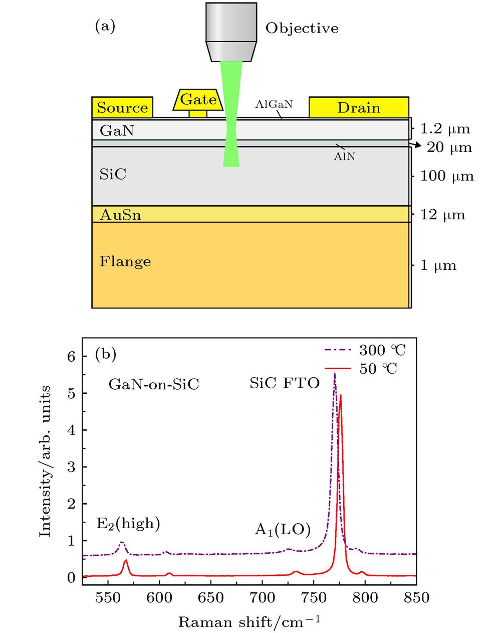
Fig. 1. (a) Schematic structure of the GaN-on-SiC HEMT under test in the Raman optothermal measurement; (b) Raman peaks of the GaN-on-SiC HEMT at 50 ℃ and 300 ℃, including the E2(high) and A1(LO) peaks of the GaN epitaxy and the FTO peak of the SiC substrate.
(a)被测GaN高电子迁移率场效应管器件结构以及拉曼热测量的示意图; (b)被测器件在50 ℃和300 ℃的拉曼特征峰: 包括GaN外延的E2(high)和A1(LO)峰, 以及SiC衬底的FTO峰
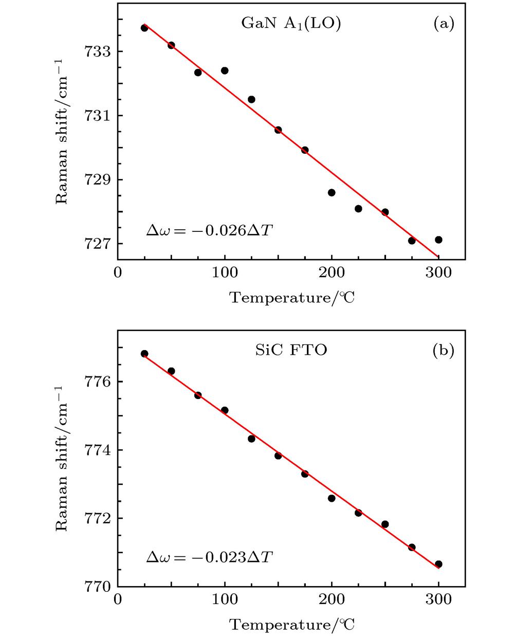
Fig. 2. (a) Position of the GaN A1(LO) Raman peak as a function of temperature. The temperature coefficient from the linear fit is –0.026 cm–1·K–1; (b) position of the SiC FTO Raman peak as a function of temperature. The temperature coefficient from the linear fit is –0.023 cm–1·K–1.
(a) GaN A1(LO)拉曼峰随温度的变化关系, 线性拟合得到的温度系数为–0.026 cm–1·K–1; (b) SiC FTO拉曼峰随温度的变化关系, 线性拟合得到的温度系数为–0.023 cm–1·K–1
Fig. 3. (a) Position of the GaN A1(LO) Raman peak as a function of the device power density. The power density coefficient from the linear fit is –1.86 cm–1·mm/W; (b) position of the SiC FTO Raman peak as a function of the device power density. The power density coefficient from the linear fit is –1.25 cm–1·mm/W.
(a) GaN A1(LO)拉曼峰随器件功率密度的变化关系, 线性拟合得到的功率系数为–1.86 cm–1·mm/W; (b) SiC FTO拉曼峰随器件功率密度的变化关系, 线性拟合得到的功率系数为–1.25 cm–1·mm/W的功率系数
Fig. 4. (a) Measured temperature of GaN, SiC, and the Cu/graphite flange as a function of the device power density; (b) temperature differences between GaN and SiC, and between GaN and and the Cu/graphite flange as a function of the device power density; (c) measured temperature of GaN, SiC, and the CuMo flange as a function of the device power density; (b) temperature differences between GaN and SiC, and between GaN and and the CuMo flange as a function of the device power density.(a)铜/石墨法兰封装器件GaN层、SiC上表层和封装法兰的温度随功率密度的变化; (b)铜/石墨法兰封装器件GaN层和SiC上表层的温度差、GaN层和封装法兰之间的温度差随功率密度的变化; (c)铜钼法兰封装器件GaN层、SiC上表层和封装法兰的温度随功率密度的变化; (d)铜钼法兰封装器件GaN层和SiC上表层的温度差、GaN层和封装法兰之间的温度差随功率密度增加的变化
Fig. 5. (a) Simulated (line) and measured (dot) junction temperatures of the Cu/graphite flanged device; (b) simulated (line) and measured (dot) junction temperatures of the CuMo flanged device; (c) depth wise temperature distribution of the Cu/graphite flanged device and the CuMo flanged device at the power density of 1.43 W/mm; (d) thermal resistance of each layer within the Cu/graphite flanged device and the CuMo flanged device (The material of TBR is AlN).(a)铜/石墨法兰封装的GaN器件的GaN外延和SiC衬底上表层温度的模拟值(线)和实测值(点); (b)铜钼法兰GaN电子器件的结温和SiC衬底上表层温度的模拟值和实测值的对比; (c) 1.43 W/mm功率密度下铜/石墨法兰和铜钼法兰封装GaN器件在垂直器件表面方向上的温度分布; (d)铜/石墨法兰和铜钼法兰封装GaN器件各层材的热阻占比(其中TBR的材料为AlN)
|
Table 1. Thermal resistance of GaN HEMT with different Cu-based flange materials.
|
Table 2. Dimensions and thermal conductivity of each layer in the GaN-on-SiC HEMT used in the finite element device thermal simulation.

Set citation alerts for the article
Please enter your email address
© Copyright 2018-2021 | Chinese Laser Press. All Rights Reserved 沪ICP备15018463号-20