Guanqi Tang, Feng Yan. Flexible perovskite solar cells: Materials and devices[J]. Journal of Semiconductors, 2021, 42(10): 101606
Search by keywords or author
- Journal of Semiconductors
- Vol. 42, Issue 10, 101606 (2021)
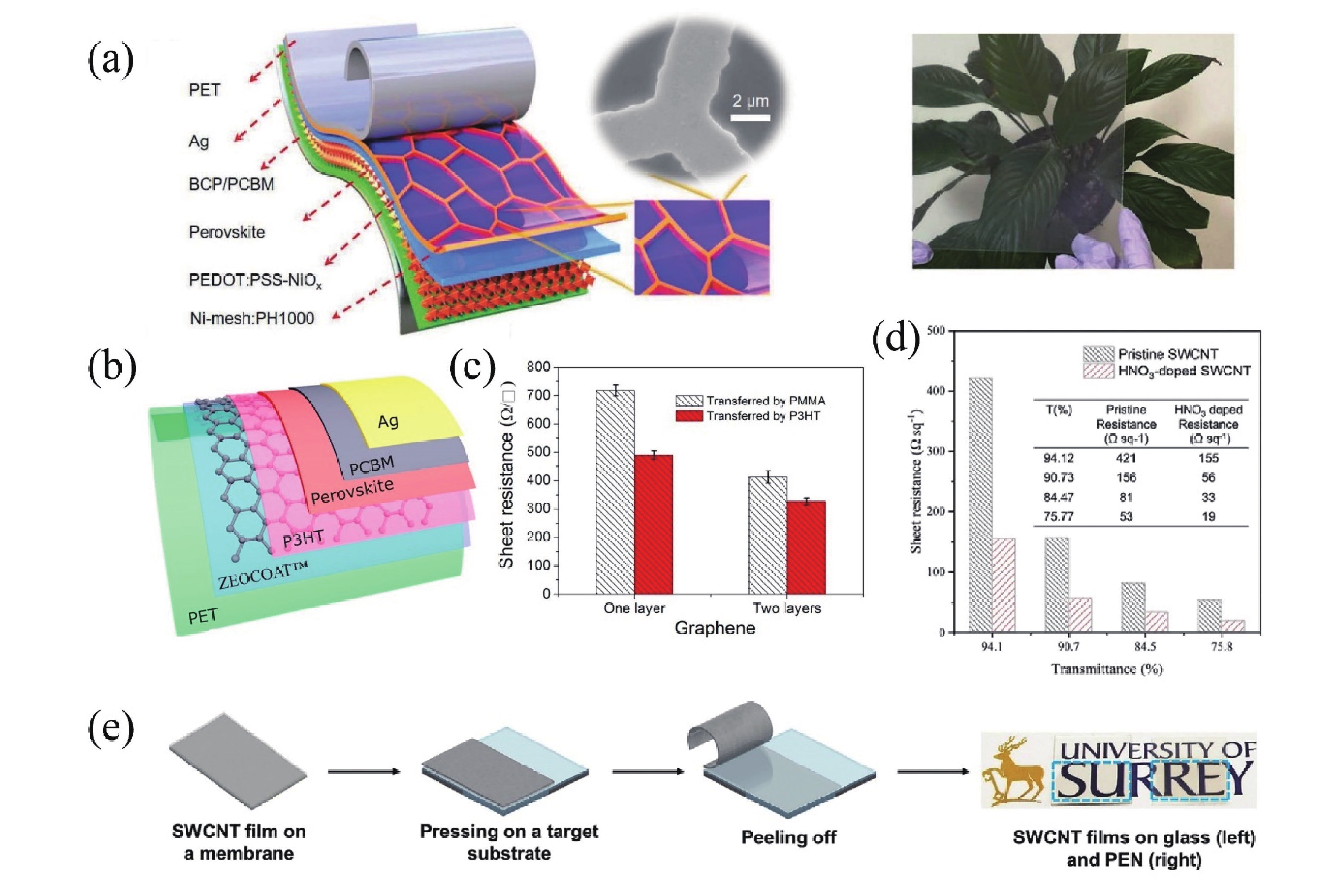
![(Color online) (a) Schematic illustration of the PET/Ni-mesh substrate, Ni-mesh:PH1000 hybrid electrode, and perovskite device; the top right image shows the SEM image of Ni-mesh. The right is the optical image of PET/Ni-mesh substrate. Reprinted with permission from Ref. [45]. Copyright 2020, John Wiley & Sons, Inc. (b) Schematic diagram of a flexible PSC with the structure of PET/graphene/P3HT/perovskite/phenyl-C70-butyric acid methylester (PCBM)/Ag. (c) The sheet resistances of one and two layers of CVD graphene transferred by using poly(methyl methacrylate) (PMMA) or P3HT. Reprinted with permission from Ref. [ 46]. Copyright 2016, Elsevier Ltd. (d) The sheet resistances of SWCNT films with different optical transmittance values before and after HNO3 treatment. (e) Dry transfer procedure of a SWCNT film and transferred SWCNT on glass and PEN substrates. Reprinted with permission from Ref. [47]. Copyright 2021, John Wiley & Sons, Inc.](/richHtml/jos/2021/42/10/101606/img_1.jpg)
Fig. 1. (Color online) (a) Schematic illustration of the PET/Ni-mesh substrate, Ni-mesh:PH1000 hybrid electrode, and perovskite device; the top right image shows the SEM image of Ni-mesh. The right is the optical image of PET/Ni-mesh substrate. Reprinted with permission from Ref. [45 ]. Copyright 2020, John Wiley & Sons, Inc. (b) Schematic diagram of a flexible PSC with the structure of PET/graphene/P3HT/perovskite/phenyl-C70-butyric acid methylester (PCBM)/Ag. (c) The sheet resistances of one and two layers of CVD graphene transferred by using poly(methyl methacrylate) (PMMA) or P3HT. Reprinted with permission from Ref. [ 46 ]. Copyright 2016, Elsevier Ltd. (d) The sheet resistances of SWCNT films with different optical transmittance values before and after HNO3 treatment. (e) Dry transfer procedure of a SWCNT film and transferred SWCNT on glass and PEN substrates. Reprinted with permission from Ref. [47 ]. Copyright 2021, John Wiley & Sons, Inc.
![(Color online) (a) TEM image of planar layer and porous planar layer coated on ITO/glass substrate and EDS mapping. (b) J–V curves of planar (green) and porous planar (orange) flexible unit cell (active area: 0.094 cm2) measured in the lab and that of Newport certification data (purple). The device based on porous planar layer exhibits a lab PCE of 20.75% and a certified PCE of 19.9%. The planar device demonstrates a PCE of 17.5%. (c) Photograph of flexible module based on porous planar CTL with an area of 400 cm2. (d) J–V curves of best-performing flexible sub-module at an aperture area of 100, 225 and 400 cm2. Reprinted with permission from Ref. [60]. Copyright 2020, Royal Society of Chemistry.](/richHtml/jos/2021/42/10/101606/img_2.jpg)
Fig. 2. (Color online) (a) TEM image of planar layer and porous planar layer coated on ITO/glass substrate and EDS mapping. (b) J –V curves of planar (green) and porous planar (orange) flexible unit cell (active area: 0.094 cm2) measured in the lab and that of Newport certification data (purple). The device based on porous planar layer exhibits a lab PCE of 20.75% and a certified PCE of 19.9%. The planar device demonstrates a PCE of 17.5%. (c) Photograph of flexible module based on porous planar CTL with an area of 400 cm2. (d) J –V curves of best-performing flexible sub-module at an aperture area of 100, 225 and 400 cm2. Reprinted with permission from Ref. [60 ]. Copyright 2020, Royal Society of Chemistry.
Fig. 3. (Color online) (a) Schematic description of perovskite film formation process by laser annealing method. Reprinted with permission from Ref. [76 ]. Copyright 2016, American Chemical Society. (b) Schematic illustration of multisource vacuum deposition with an in-vacuum annealing process for large-area perovskite films. Photographs of FA-based perovskite films deposited on (c) glass and (d) PET substrates. Reprinted with permission from Ref. [77 ]. Copyright 2021, Royal Society of Chemistry. (e) Cross-section SEM images of an FPSC with a structure of PEN/ITO/SnO2/3D/2D perovskite/ Spiro-OMeTAD/Ag and J –V curves of 3D and 2D/3D FPSCs. Reprinted with permission from Ref. [20 ]. Copyright 2021, John Wiley & Sons, Inc. (f) Schematic illustrate of the interaction between s-GO with perovskite. (g) Schematic diagram of the enhanced water resistance with flexural endurance due to cementation and passivation of grain boundaries. Reprinted with permission from Ref. [ 78 ]. Copyright 2020, Elsevier Ltd.
Fig. 4. (Color online) (a) Diagram showing R2R processing for the fabrication of FPSCs. (b) Photograph of fully R2R processed PSCs. (c) The J –V curves of fully R2R gravure-printed PSCs. Reprinted with permission from Ref. [24 ]. Copyright 2020, Nature Publishing Group.
Fig. 5. (Color online) (a) Photographs of silk derived electrodes using natural silkworm cocoons as raw materials, which show high transmittance and various deformation including wave, spiral, bowknot, flower and paper crane. Reprinted with permission from Ref. [91 ]. Copyright 2020, John Wiley & Sons, Inc. (b) Schematic illustration of the stretching process of the kirigami structure at left) initial state and right) stretching state. (c) Voltage response of kirigami-based PSCs in a stretching cycle. Reprinted with permission from Ref. [ 92 ]. Copyright 2020, American Chemical Society. (d) Digital photographs demonstrating left) the integrating process of the self-powered smart bracelet and right) a subject wearing the self-powered smart bracelet on wrist during outdoor running and indoor biking. Reprinted with permission from Ref. [17 ]. Copyright 2021, American Chemical Society. (e) A photo of a solar powered wearable sensor. Reprinted with permission from Ref. [25 ]. Copyright 2019, Elsevier Ltd.

Set citation alerts for the article
Please enter your email address


