Hao Ma, Yuanan Zhao, Jianda Shao. Fabrication and Application of All-Dielectric Nanoparticles[J]. Laser & Optoelectronics Progress, 2019, 56(9): 090004
Search by keywords or author
- Laser & Optoelectronics Progress
- Vol. 56, Issue 9, 090004 (2019)
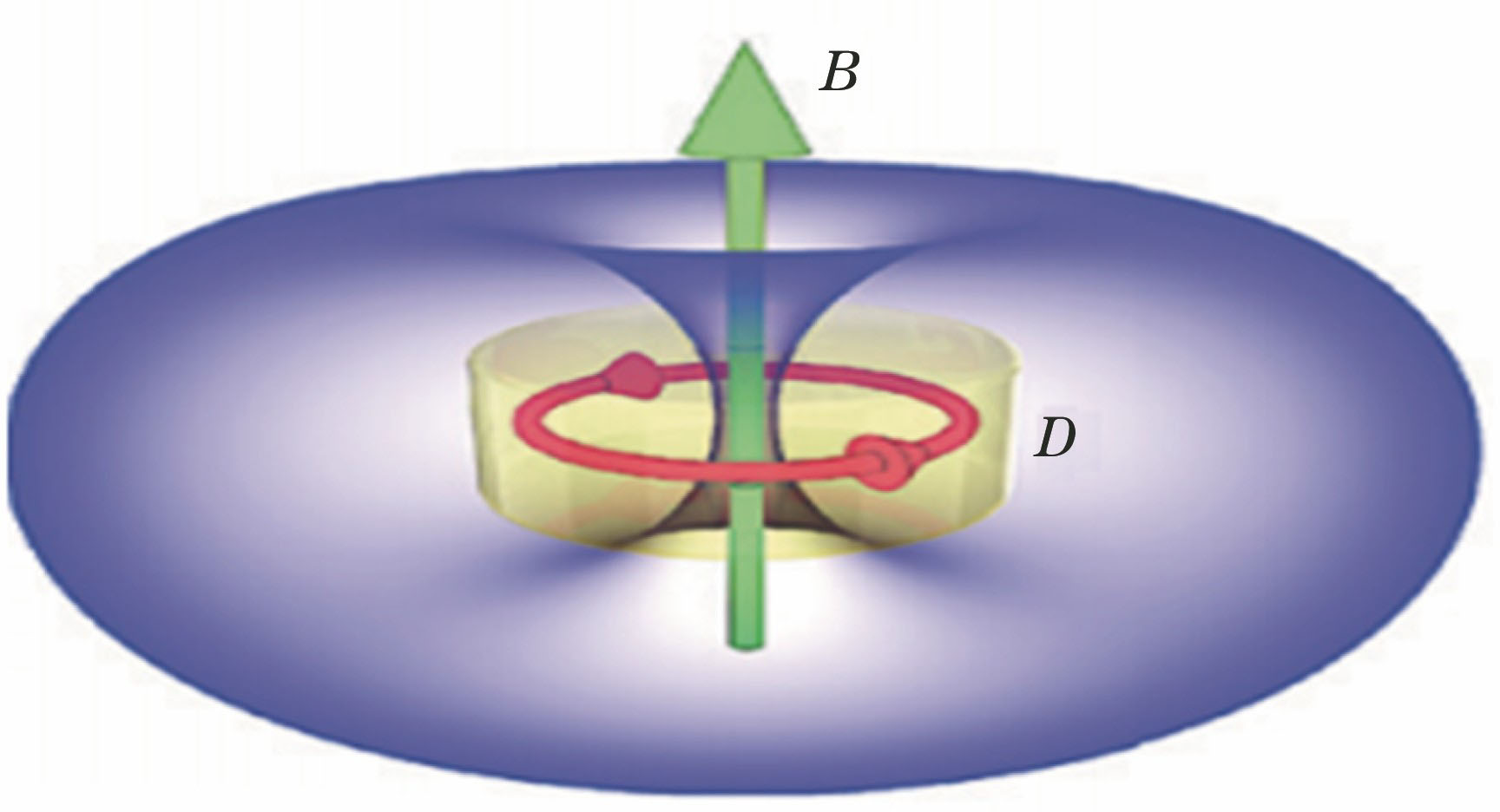
![Schematic of magnetic-dipole moment excited in all-dielectric nanoparticles[35]](/richHtml/lop/2019/56/9/090004/img_1.jpg)
Fig. 1. Schematic of magnetic-dipole moment excited in all-dielectric nanoparticles[35]
![Spectral dependence properties of crystalline silicon at room temperature[36]. (a) Real and imaginary parts of refractive index; (b) ratio between electrical conduction current and displacement current](/richHtml/lop/2019/56/9/090004/img_2.jpg)
Fig. 2. Spectral dependence properties of crystalline silicon at room temperature[36]. (a) Real and imaginary parts of refractive index; (b) ratio between electrical conduction current and displacement current
Fig. 3. Electric field distributions in nanoparticles under different conditions. (a) MD resonance; (b) ED resonance
Fig. 4. Examples of high-index dielectric nanoparticles fabricated by lithography. (a) Scanning electron microscopy (SEM) image of hollow Si cylinder[38]; (b) Si nanoparticles obtained by means of reactive-ion-etching based on mask[39]; (c) Si nanoparticles with additionally deposited Si3N4 thin film[40]
Fig. 5. SEM images of Si colloids and Si nanoparticles. (a) High-magnification SEM images of silicon colloids [41]; (b) self-aligned silicon nanoparticles obtained by chemical deposition[43]
Fig. 6. Dark-field optical image of Si nanoparticles and atomic force microscope (AFM) image of SiGe nanoparticles. (a) Dark-field optical image of Si nanoparticles obtained by thin film dewetting[44]; (b) AFM image of SiGe nanoparticles in array received after thermal dewetting[46]
Fig. 7. Examples of high-index dielectric nanoparticles fabricated by laser ablation method. (a) Dark-field optical image of silicon nanoparticle obtained via femtosecond laser ablation of bulk silicon[47]; (b) transmission electron microscope (TEM) image of ZnO submicrosphere[48]; (c) TEM image of CdSe submicrosphere[48]
Fig. 8. Examples of silicon nanoparticles fabricated by LIT method[50]. (a) Array of amorphous Si nanoparticles fabricated by LIT method and visualized with dark-field microscopy; (b) femtosecond laser printed Si nanoparticles
Fig. 9. Resonant characteristics of nano-resonators with high index semiconductor materials. (a) Cubic, spherical or disc-shaped resonators composed of high-index dielectric[52]; (b) effective negative magnetic permeability μeff and e?ective negative dielectric permittivity εeff52; (c) reflection and transmission spectra of two-dimensional arrays of tellurium resonators near electric or magnetic resonance[21]
Fig. 10. Wavelength dependence of directivity of two types of all-dielectric nano-antennas[67]. (a) Single dielectric nanoparticle; (b) Yagi-Uda-type structure when separation distance D is 70 nm
Fig. 11. Maximum directivity of super-directive nano-antenna versus position of dipole source at wavelength of 455 nm[68]
Fig. 12. Several common metamaterial structures. (a)(b) All-dielectric metamaterial based on spherical and cylindrical particles[77] ; (c)-(f) all-dielectric metasurfaces[78,57,40]
Fig. 13. Spectrum for third harmonic generation (THG) of Si nanodisk array and directionality of Si nano-antenna. (a) THG spectrum of nanodisk array(purple dots)and linear transmission spectrum (gray area) [26]; (b)dynamical reconfiguration of Si nano-antenna directivity via photoexcitation, and scattering diagrams of incident beam at largest intensity shown in two insets[29]

Set citation alerts for the article
Please enter your email address


