
Xiaobin Liu, Xuetong Li, Yuxuan Li, Yingzhi Li, Zihao Zhi, Min Tao, Baisong Chen, Lanxuan Zhang, Pengfei Guo, Guoqiang Lo, Xueyan Li, Fengli Gao, Bonan Kang, Junfeng Song, "Three-terminal germanium-on-silicon avalanche photodiode with extended p-charge layer for dark current reduction," Photonics Res. 10, 1956 (2022)
- Photonics Research
- Vol. 10, Issue 8, 1956 (2022)
![(a) Structural diagram of three-terminal Ge-on-Si APD. (b) SEM image of pixel units. (c) Electric field simulation diagram of Ge region. (d) Simulated electric field in Si APD area [electric field at different positions of line A in (b)].](/richHtml/prj/2022/10/8/1956/img_001.jpg)
Fig. 1. (a) Structural diagram of three-terminal Ge-on-Si APD. (b) SEM image of pixel units. (c) Electric field simulation diagram of Ge region. (d) Simulated electric field in Si APD area [electric field at different positions of line A in (b)].
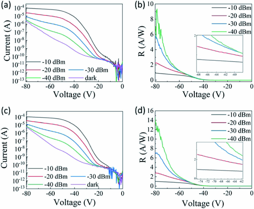
Fig. 2. (a) Current characteristic diagram at 1550 nm under different input optical power. (b) Responsivity characteristic diagram at 1550 nm under different input optical power. (c) Current characteristic diagram at 1310 nm under different input optical power. (d) Responsivity characteristic diagram at 1310 nm under different input optical power. The figure shows the voltage applied to two terminals Ge and n + +
Fig. 3. It represents the simulated dark current diagram (current output at the n + + n + + p + +
Fig. 4. When the n + + p + + − 20 dBm n + + − 20 dBm
Fig. 5. (a) Schematic diagram of three-terminal APD. (b) Y B B ′ X A A ′
Fig. 6. (a) Photocurrent diagram at 10 − 7 A 10 − 7 A 10 − 8 A 10 − 8 A
Fig. 7. When the voltage on Ge is − 27.5 V
Fig. 8. When the voltage on Ge is − 27.5 V
Fig. 9. When the applied voltage on p + + − 27.5 V − 20 dBm
Fig. 10. (a) Current at − 20 V − 25 V − 30 V
Fig. 11. (a) The APD has a normalized RF response characteristic at a voltage of Ge at − 27.5 V − 27.5 V
Fig. 12. (a) When the voltage is − 27.5 V
|
Table 1. Response of Ge to −27.5 V at Different Input Power
|
Table 2. Fitted Electric Circuit Parameters of a Three-Terminal Avalanche Photodiode under a Reverse Bias of 15 V
|
Table 3. Device Performance of Surface Illuminated APDs


Set citation alerts for the article
Please enter your email address

© Copyright 2018-2021 | Chinese Laser Press. All Rights Reserved 沪ICP备15018463号-20