
L. Castañeda. Transparent conductive stannic oxide coatings employing an ultrasonic spray pyrolysis technique: The relevance of the molarity content in the aerosol solution for improvement the electrical properties[J]. Journal of Semiconductors, 2022, 43(2): 022802
- Journal of Semiconductors
- Vol. 43, Issue 2, 022802 (2022)
Abstract
1. Introduction
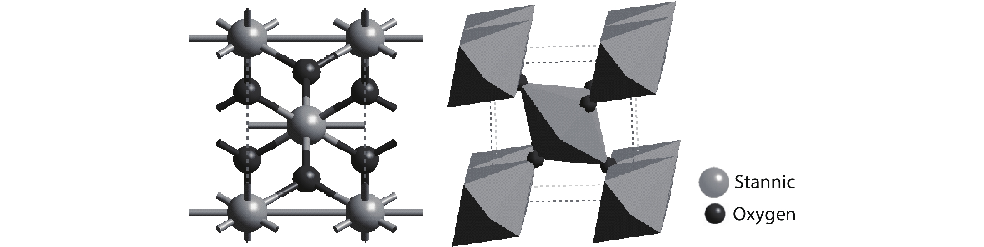
The stannic oxide (SnO2) is an “n-type” semiconducting material with a crystal structure of rutile (tetragonal), crystal classification of ditetragonal dipyramidal (4/mmm), and H-M symbol of (4/m 2/m 2/m). The space group is P42/mnm, Pearson's symbol or Pearson's notation is tP6, so that the stannic oxide is in the crystalline phase that has a tetragonal structure of the rutile type. The unit cell has six atoms, including two stannum, and four oxygen atoms (see Fig. 1). Stannic oxide has a wide band gap approximately of 3.7–4.0 eV[
![]()
Figure 1.Crystal structure and coordination polyhedron of the stannic oxide (cassiterite).
Our main interest is to deposit stannic oxide (SnO2) coatings that are arranged with different molarities of the aerosol solution via an environmentally benign chemical route, it is permitted to see an ultrasonic spray pyrolysis procedure, and implementing their electrical, morphological, and optical properties.
2. Experimental details
2.1. Experimental setup to prepare the nanocrystalline stannic oxide coatings
Fig. 2 shows the scheme of the experimental arrangement occupied for the deposition process of the stannic oxide coatings by the ultrasonic spray pyrolysis method (UPS) for the preparation of the SnO2 coatings. The system contains a spraying chamber was made of clear quartz plain, an ultrasonic generator, a spray faucet (Sono-Tek) attached to an x-y printer, a syringe siphon pump, a heating system with a bronze hunk, and temperature display. The ultrasonic generator created high-frequency ultrasonic waves with a frequency of 140 kHz. This high-frequency signal was exercised to the piezoelectric transducer coupled with the faucet. The piezoelectric transducer transforms a high-frequency signal in the direction of through to mechanical energy. This energy is active to transfer the aerosol solution and maintains a very fine mist.
![]()
Figure 2.(Color online) Illustration of the experimental method employed for the deposition process of the stannic oxide coatings by the USP.
2.2. Cleaning process of the Corning® EAGLE XG®slim glass and silicon single-crystal wafers
The coatings were deposited on top of Corning® EAGLE XG® slim glass substrates (1.0 × 1.0 × 0.2 in3) which were previously cleansed as follows: (i) a five-minute ultrasonic bath in trichloroethylene (C2HCl3) (98%, from J.T. Baker, Naucalpan, Edo. Mex., Mexico) was implemented to degrease the substrates, followed by (ii) a five minutes bath in a methyl alcohol [CH3OH] (98%, from J.T. Baker, Naucalpan, Edo. Mex., Mexico); (iii) a five-minute ultrasonic bath in acetone (CH3COCH3)(98%, from J.T. Baker, Naucalpan, Edo. Mex., Mexico); and finally, (iv) the substrates were dried by a jet of pure and dry nitrogen (N2) (98%, from PRAXAIR, Ciudad de México, México). For ellipsometry measures, the coatings were deposited on n-type (100) “n-type” silicon single-crystal wafers of 200 Ω·cm (from Sigma-Aldrich, Química, S.L. Toluca, México). It is very important that the wafers are free of all organic residues, and surface particles are removed. Cleaning is accomplished by a thorough “P” solution rinse followed by baking at temperatures between 393.15–473.15 K for up to 1200.0 s. To remove the native oxide from the silicon wafers, they were chemically etched with “P” solution (15.0 parts of hydrogen fluoride (HF) (99.999%, from Sigma-Aldrich, Química, S.L. Toluca, México) 10.0 parts of nitric acid (HNO3) (99.999%, from Sigma-Aldrich, Química, S.L. Toluca, México) and 300.0 parts of deionized water [H2O] (Resistivity of water produced at ~296.15 K, > 5.0 MΩ·cm, ZLXL62080 Milli-Q, from Merck Milipore, México).
2.3. Preparation of the stannic oxide coatings
Transparent conductive stannic oxide coatings were processed from the solution and prepared by dissolving stannous chloride or tin(II) dichloride dihydrate (SnCl2·2H2O) (98% from Alfa Aesar, Ward Hill, MA, USA) to dissolve in deionized water (H2O) (Resistivity of water produced at ~296.15 ± 0.05 K > 5.0 MΩ·cm, ZLXL62080 Milli-Q, from Merck Milipore, México) to get 0.05, 0.15, 0.20 and 0.30 M concentration of aerosol solutions. If we define molarity as a measure of the concentration of a solute in a solution, be it some molecular, ionic or atomic species. Since volume is temperature-dependent, the problem is usually solved by introducing temperature correction factors or coefficients, or by using temperature-independent concentration measures such as molality.
The concentration or molarity, represented by the letter M, is defined as the amount of solute (expressed in moles) per liter of solution, or per unit of available volume of the species:
where n is the amount of solute in moles, m is the mass of solute expressed in grams, PM is the molar mass expressed in g/mol, and V is the volume in liters of the solution.
For removing any precipitate in solution, 10.0 ± 0.5 mL of hydrochloric acid [HCl] (99% from Alfa Aesar, Ward Hill, MA, USA) was added. The mixture was vigorously stirred at 873.15 K for approximately one hour. The mist formed by the faucet was atomized on the Corning® EAGLE XG® slim glass substrates and “n-type” (100) silicon wafers. The substrates were then placed in an employed tin bath, and the temperature was measured just below the substrate using a thin chromel–alumel thermocouple contained in a stainless steel metal jacket. The substrate temperature was 623.15 ± 0.05 K. Nitrogen (N2) (99.99%, from PRAXAIR, Ciudad de México, México) was employed one and the other as the aerosol solution carrier as well as aerosol directing gas, maintaining its flow rates at 3500 and 500 mL/min, correspondingly. The deposition time was set to 10.0 ± 0.1 min. It is also worth mentioning that the pH of the solutions varied from 4.5 to 4.0, depending on the molarity concentration (pH = 4.5 and pH = 4.0 were observed for the extreme cases when 0.05 and 0.30 M concentration of aerosol solutions, respectively). These measurements were carried out using a SevenExcellence pH meter S400 METTLER TOLEDO. With an accuracy of the 1.0 %.
2.4. Analysis of the transparent conductive stannic oxide coatings
The morphology of the coatings was observed by scanning electron microscopy (SEM) using a Philips emission field XL-30 operated at 20 kV. The structure of the deposited SnO2 coatings was determined through X-ray diffraction (XRD) using the θ–2θ method on a GBC-MMM diffractometer (GBC Scientific Equipment Pty Ltd 2003) using Cu Kα1 (λ = 0.15405 nm) radiation, with a scanning range from 2θ = 20° to 80° with a step interval of 0.01° in 2θ degrees. The accelerating voltage was set at 45 keV with a 28.5 mA flux. Scatter and Soller slit and divergence slit D1, and 3.93 × 10⁻³ inch collection slit were employed. Instrumental broadening was measured for lanthanum hexaboride (LaB6). The contribution of Kα2 was subtracted from the peak profile, and Lorentzian fitting was performed, resulting in a 2θ broadening of 0.05. The average dimensions of the crystallites size were calculated using Debye-Scherer formula. The thickness and roughness of the coatings were measured using a KLA profilometer (Tencor model P15 with an uncertainty of ±0.05° nm) on the step formed immediately after deposition.
The optical absorption of the coatings was measured using a UV–visible spectrophotometer Shimadzu 2450 UV–VIS (with an uncertainty of ±0.05° nm). The refractive index n was measured with a Gaertner L-117A ellipsometer at a wavelength of 632 nm using a He–Ne laser (with an uncertainty of ±0.5°nm). Ellipsometry is the best applicable for measuring the optical constants of the coatings. Optical characterization of the SnO2 samples was carried out using optical transmittance spectra in the 190–1050 nm range using a double-beam Shimadzu UV–Vis (model 260 spectrophotometer, with an uncertainty of ±0.5°nm) and taking into account the air in the reference beam. The photoluminescence (PL) spectra of the samples were obtained from 300 to 900 nm using an excitation line at λ = 300 nm (FluoroMax-3, Jobin-Yvon-Horiba PL-system). The Hall Effect measurement systems using an ECOPIA HMS-5000 in van der Pauw configuration were employed to tailor the electrical properties of the deposited coatings. Illumination of the as-prepared samples was performed using a halogen reflector lamp (300 W/82 V) for photoconductivity (pc) excitation spectrum measurements, and the photocurrent was continuously recorded using a 2450 Keithley source meter. The electrical sheet resistance was determined using a four-point probe arrangement (Veeco Model FPP-100 equipment, using appropriate correction factors contained in the reference manual).
3. Results and discussion
3.1. Structural analysis of the transparent conductive stannic oxide coatings
The X-ray diffraction patterns of the corresponding samples exhibited a polycrystalline character, irrespective of the deposition conditions. Fig. 3(a) shows the XRD patterns of SnO2 coatings, in which the major diffraction peaks correspond to the (112), (006), (122), (188), (133), and (312) family planes of the orthorhombic phase, in agreement with the standard JCPDS file no: 78-1063.
![]()
Figure 3.(Color online) (a) XRD patterns and (b) Williamson–Hall plot of the as grown samples.
The crystallite size was estimated using the (112), (006), (122), (188), (133), and (312) diffraction peaks from the XRD data in accordance with the Debye–Scherer formula[
where D is the crystallite size in nanometers, λ is the wavelength of the Cu Kα1 line, θ is the Bragg diffraction angle, and B is the FWHM of the diffraction peak measured in radians. The dislocation density (δ), which measures the length of dislocation lines per unit volume (lines/m2), is calculated using the following relation[
The diffraction line broadening employed by the strain and reduced grain size was analyzed using the Williamson–Hall (W–H) method. The relation employed for the calculation of lattice strain and crystallite size[
where ξ is the lattice strain. The average grain size was evaluated using the Debye–Scherer formula and W–H plot of pristine SnO2 samples. The results are shown in Table 1. With an accuracy of the 5%. It is observed that 0.05 and 0.15 M SnO2 coatings show lattice elongation and 0.20 and 0.30 M the stannic oxide coatings show lattice compression.
The reflection intensities from each of the X-ray diffraction patterns contain information related to the preferential or random growth of polycrystalline thin films using the following expression[
where Tc(hkl) corresponds to the texture coefficient, I(hkl) indicates the X-ray diffraction intensities obtained from the films, and n is the number of diffraction peaks considered. Ir(hkl) is the intensity of the reference diffraction pattern (which has been obtained from the ASTM SnO2 card). Table 2 shows the texture coefficients of each (hkl) plane. The deviation of the texture coefficient from unity indicates the preferred orientation of the growth. The more the texture coefficient deviates from unity, the higher the preferred orientation of the film. It is clear that (112) has a highly preferred orientation for all samples.
3.2. Morphological studies
The morphologies of the stannic oxide coatings are shown in Fig. 4. The SnO2 coatings produced with 0.05 M aerosol exhibits fine particles on the surface. When the aerosol morality becomes 0.15, the stannic oxide grows in size with an irregular shape, and for higher molarities the particles look like rice grains and are irregularly distributed and densely packed over the surface. It was found that the grain size increased with molarity and the 0.2 M sample had the maximum surface smoothness.
![]()
Figure 4.Scanning electron microscope images of the stannic oxide coatings for different molarities (a) 0.05 M, (b) 0.15 M, (c) 0.20 M and (d) 0.30 M.
3.3. Ellipsometry and profilometry studies
The refractive index and extinction coefficient of the coatings were determined using ellipsometry analysis. The thickness and roughness of the samples were measured using profilometry. If the mean square error (MSE) is less than 10, it can be judged as the high quality of the coatings, and in the present study, all the samples possess MSE < 10. Table 3 shows the ellipsometry data for the as-prepared SnO2 samples. The thickness of the coatings varies in the 70–150 nm range. The explanation is due to the increased thickness of the sample when increased molarity in the aerosol solution. Fig. 5(a) shows the change in thickness and roughness with doping concentration, and Fig. 5(b) shows the variation in the refractive index and extinction coefficient at 632.8 nm with the molarity concentration in the aerosol solution.
![]()
Figure 5.(Color online) (a) Variation of thickness and roughness of coatings with doping and (b) variation of refractive index and extinction coefficient of films at 632.8 nm with doping concentration.
3.4. Optical properties
Fig. 6(a) shows the transmission spectra of the pristine SnO2 coatings for different molarities of the aerosol solution. The transmission percentage varied with molarity, and all samples showed constant transmission over the entire visible region. A maximum of approximately 60% transmission is observed for the film with 0.20 M a concentration.
![]()
Figure 6.(Color online) (a) Transmission spectra and (b) Tauc plot of pristine SnO2 coatings.
The determination of the band gap is an important aspect for characterizing the sample. Here, a Tauc plot is employed to find the band gap using the relation proposed by Tauc, Davis, and Mott[
where hυ refers to the photon energy and α is the absorbance. The optical band gap was determined by extrapolating the linear portion of the (αhυ)2 vs hυ curve to the x-axis (Fig. 6(b)).
The band gap values vary from 3.26 to 3.75 eV for as prepared samples from various concentrations. With an accuracy of the 1.0%. It can be observed that the band gap varies in accordance to the carrier concentration, as shown in Table 5, which is due to the BM effect. For the samples synthesized at 0.05 and 0.15 M, the band gap is less than the bulk value (3.6 eV) showing a band tailing effect. Fig. 6(b) shows that the band gap increases with molarity.
3.5. Photoluminescence studies
The photoluminescence (PL) spectra of the as-grown samples are depicted in Fig. 7(a).
![]()
Figure 7.(Color online) (a) Photoluminescence spectra and (b) Commission Internationale de l'éclairage (CIE) diagram of the SnO2 coatings for different molarities.
The photoluminescence spectra of the samples were found to possess two broad emissions, which correspond to near-band-edge emission (NBE) and deep-level emission (DLE) in the region 380–620 nm, with an accuracy of 1.0%.
Generally, NBE emission is due to excitons, and DLE is due to intrinsic and extrinsic defects. The NBE emission observed in all the samples was located at 396 nm. It is observed that the NBE emission intensity increases with molarity, with small shifts in the peak center.
The oxygen vacancies present in the samples acted as luminescent centers. Oxygen vacancies can be neutral (VO0), singly charged (VO+), or doubly charged (VO2+)[
3.6. Electrical studies
The electrical properties of the samples were characterized at room temperature using Hall problem measurements in a Van der Pauw configuration. All SnO2 coatings showed n-type conduction owing to the presence of oxygen vacancies. The mobility, carrier concentration, the hole concentration in the valence band, and resistivity of the samples are shown in Table 5.
It was observed that the carrier concentration increased and the mobility decreased with increasing molarity of the aerosol solution. Fig. 8(a) shows the change in conductivity and mobility with the molarity of the aerosol solution. The conductivity of the films increased with increasing molarity up to 0.2 M and then decreases. This is in accordance with the variation in the intensity of the DLE emission in the PL spectra.
![]()
Figure 8.(Color online) (a) Variation of conductivity, and mobility with molarity of aerosol solution and (b) Arrhenius plot of SnO2 coating from 0.2 M in the aerosol solution.
It is appropriate to plot the logarithm of the conductivity (ln σ) as a function of 1000/T to analyze the conductivity mechanism. Fig. 8(b) shows the Arrhenius plot of the SnO2 sample from 0.2 M aerosol solution at different temperatures in the range 308–423 K. From the figure, it is clear that all the samples exhibit semiconducting behavior. The activation energy Ea was calculated from the slope of the Arrhenius plot[
3.7. Transient photoconductivity studies
To check the photodetector applicability of the SnO2 coatings, the samples were illuminated using a halogen reflector lamp. All the synthesized SnO2 coatings considered in the present study have a photocurrent more than the dark current and hence show positive photoconductivity. This is due to the absorption of photons by the mobile charge carriers present in the samples[
![]()
Figure 9.Transient photoconductivity of as grown SnO2 coatings for different molarities (a) 0.05 M, (b) 0.15 M, (c) 0.20 M and (d) 0.30 M.
The dark current was measured for up to 100 s and then the sample was illuminated by a halogen reflector lamp. Upon illumination, the photocurrent initially increased in all samples. This may be due to the fast production of electron–hole pairs as a result of photon absorption. The photocurrent decreases exponentially within a few seconds after the illumination of the coatings, as shown in Fig. 9.
The dark current was measured for up to 100 s, and then the sample was illuminated by a halogen reflector lamp. Upon illumination, the photocurrent initially increased in all coatings. This may be due to the fast production of electron–hole pairs as a consequence of photon absorption. The photocurrent decreases exponentially within a few seconds after the illumination is switched off and attains a constant value after a long time. The decrease in the photocurrent is due to the recombination of electron–hole pairs with each other and is captured by re-adsorbed oxygen molecules[
4. Conclusions
The molarity of the aerosol solution affects the properties of the SnO2 coatings prepared by ultrasonic spray pyrolysis. The ellipsometry and profilometry studies showed the high-quality of the coatings, as all the samples possess MSE < 10 and the sample prepared at 0.2 M concentration of aerosol solution has minimum MSE and surface roughness values. A maximum transmission of 60% in the visible region, a maximum conductivity of 24.86 S/cm and moderate mobility of 5.2 cm 2/(V·s) were shown by 0.2 M sample. The results suggest that SnO2 coatings with a 0.20 M aerosol solution could be employed as the n-layer in the p-n junction diode. An important factor in these developments was that the quality and availability of stannic oxide coatings have dramatically improved in recent years, and that high-quality epitaxial layers are now being controllably produced. Still, a number of areas need more investigations; in particular, we note the possible presence of an electron accumulation layer on the surface, and its effects on measurements of conductivity of the underlying layers. A pragmatic synergism between theory and experiment could greatly aid in achieving the desired objectives.
Acknowledgements
The authors would like to thank the financial support from the Escuela Superior de Medicina, Instituto Politécnico Nacional, through Project No. 20210385.
References
[1] L Castañeda. Present status of the development and application of transparent conductors oxide thin solid films. Mater Sci Appl, 2, 1233(2011).
[2] . Study of porous nanoflake ZnO for dye-sensitized solar cell application. Am J Eng Appl Sci, 2, 236(2009).
[3] L Castañeda, M Avendaño-Alejo. Physical characterization of nickel-doped zinc oxide thin solid films deposited by the ultrasonic chemically sprayed technique: Gas-sensing performance in a propane atmosphere. J Nanoelectron Optoelectron, 9, 419(2014).
[4] L Castañeda, A Maldonado, J Rodríguez-Baez et al. Chemical spray pyrolysis deposited fluorine-doped zinc oxide thin films: Effect of acetic acid content in the starting solution on the physical properties. Mater Sci Semicond Process, 15, 232(2012).
[5] L Castañeda, O G Morales-Saavedra, D R Acosta et al. Structural, morphological, optical, and nonlinear optical properties of fluorine-doped zinc oxide thin films deposited on glass substrates by the chemical spray technique. Phys Status Solidi A, 203, 1971(2006).
[6] M Suchea, S Christoulakis, K Moschovis et al. ZnO transparent thin films for gas sensor applications. Thin Solid Films, 515, 551(2006).
[7] L Castañeda. Evaluating propane sensing properties of ultrasonic spray deposited zinc oxide thin solid films. J Nanoelectron Optoelectron, 13, 819(2018).
[8] S Hussain, T M Liu, N Aslam et al. Polymer-assisted co-axial multi-layered circular ZnO nanodisks. Mater Lett, 152, 260(2015).
[9] S Hussain, T M Liu, M Kashif et al. A simple preparation of ZnO nanocones and exposure to formaldehyde. Mater Lett, 128, 35(2014).
[10] L Castañeda. The effects of warmness plasma, and high frequency electrical field on beam-1 plasma interaction in plasma waveguide. J Comput Theor Nanosci, 15, 1830(2018).
[11] M Girtan, G G Rusu, S Dabos-Seignon et al. Structural and electrical properties of zinc oxides thin films prepared by thermal oxidation. Appl Surf Sci, 254, 4179(2008).
[12] J S Lee, M S Islam, S Kim. Photoresponses of ZnO nanobridge devices fabricated using a single-step thermal evaporation method. Sens Actuators B, 126, 73(2007).
[13] L Castañeda, M Avendaño-Alejo, H Gómez et al. Physical characterization of ruthenium-doped zinc oxide thin solid films deposited by the sol–gel technique: Gas-sensing performance in a propane atmosphere. Sen Lett, 11, 286(2013).
[14] L Castañeda. Synthesis and characterization of ZnO micro- and nano-cages. Acta Mater, 57, 1385(2009).
[15] C H Ku, J J Wu. Chemical bath deposition of ZnO nanowire–nanoparticle composite electrodes for use in dye-sensitized solar cells. Nanotechnology, 18, 505706(2007).
[16] L Castañeda. Photoluminescence and morphological characterization of silver-doped zinc oxide novel nanostructures obtained by ultrasonic spray pyrolysis. J Nanoelectron Optoelectron, 8, 373(2013).
[17]
[18] L Castañeda, C Torres-Torres, M Trejo-Valdez et al. Optical and photoconductive properties exhibited by silver doped zinc oxide thin films. J Nanoelectron Optoelectron, 8, 267(2013).
[19]
[20] S Park. Enhancement of hydrogen sensing response of ZnO nanowires for the decoration of WO3 nanoparticles. Mater Lett, 234, 315(2019).
[21] A Aziz, N Tiwale, S A Hodge et al. Core-shell electrospun polycrystalline ZnO nanofibers for ultra-sensitive NO2 gas sensing. ACS Appl Mater Interfaces, 10, 43817(2018).
[22] M Jeem, L H Zhang, J Ishioka et al. Tuning optoelectrical properties of ZnO nanorods with excitonic defects via submerged illumination. Nano Lett, 17, 2088(2017).
[23] R Zhu, W G Zhang, C Li et al. Uniform zinc oxide nanowire arrays grown on nonepitaxial surface with general orientation control. Nano Lett, 13, 5171(2013).
[24] T Y Zhai, L Li, Y Ma et al. One-dimensional inorganic nanostructures: Synthesis, field-emission and photodetection. Chem Soc Rev, 40, 2986(2011).
[25] J N Ding, Y R Zhou, G Q Dong et al. Solution-processed ZnO as the efficient passivation and electron selective layer of silicon solar cells. Prog Photovolt: Res Appl, 26, 974(2018).
[26] P L Chen, X Y Ma, D R Yang. Ultraviolet electroluminescence from ZnO/p-Si heterojunctions. J Appl Phys, 101, 053103(2007).

Set citation alerts for the article
Please enter your email address
© Copyright 2018-2021 | Chinese Laser Press. All Rights Reserved 沪ICP备15018463号-20