• Journal of Infrared and Millimeter Waves
  • Vol. 41, Issue 6, 1009 (2022)
Hui QIAO, Ni-Li WANG, Tian-Yi LAN, Shui-Ping ZHAO, Qi-Zhi TIAN, Ye LU, Reng WANG, Qin HUO, Fan SHI, Yi-Dan TANG, Kai-Hui CHU, Jia JIA, Qing ZHOU, Xiao-Yu SUN, Pei-Lu JIANG, Yi LUO, Xin-Yi CHENG, and Xiang-Yang LI*
Author Affiliations
  • Key Laboratory of Infrared Imaging Materials and Detectors,Shanghai Institute of Technical Physics,Chinese Academy of Sciences,Shanghai 200083,China
  • show less
    DOI: 10.11972/j.issn.1001-9014.2022.06.010 Cite this Article
    Hui QIAO, Ni-Li WANG, Tian-Yi LAN, Shui-Ping ZHAO, Qi-Zhi TIAN, Ye LU, Reng WANG, Qin HUO, Fan SHI, Yi-Dan TANG, Kai-Hui CHU, Jia JIA, Qing ZHOU, Xiao-Yu SUN, Pei-Lu JIANG, Yi LUO, Xin-Yi CHENG, Xiang-Yang LI. Failure modes and analysis for HgCdTe linear photoconductive detectors[J]. Journal of Infrared and Millimeter Waves, 2022, 41(6): 1009 Copy Citation Text show less
    The schematic diagram of HgCdTe photoconductive detector (a) side view, (b) vertical view, (c) vertical view of serpentine geometry pixel, (d) side view of overlap contact geometry
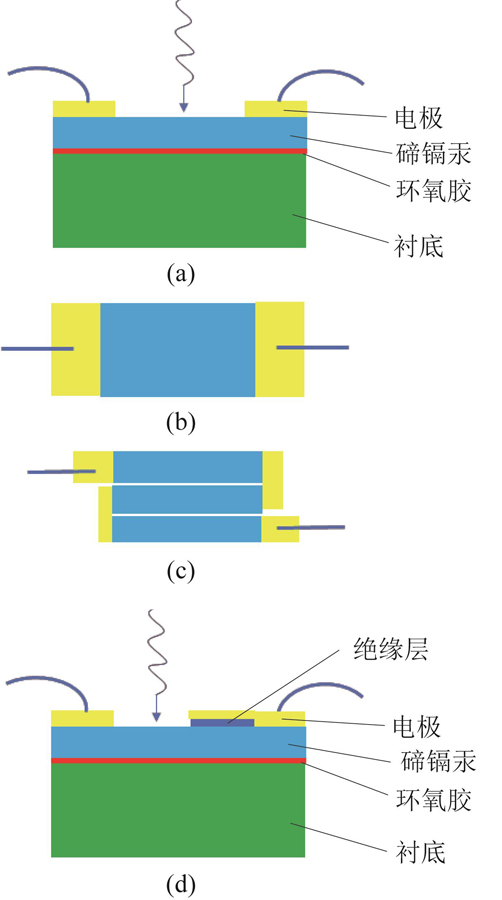
    Fig. 1. The schematic diagram of HgCdTe photoconductive detector (a) side view, (b) vertical view, (c) vertical view of serpentine geometry pixel, (d) side view of overlap contact geometry
    Photographs of HgCdTe photoconductive detector with two kinds of pixel geometry
    Fig. 2. Photographs of HgCdTe photoconductive detector with two kinds of pixel geometry
    Diagram of FTIR spectrum of HgCdTe photoconductors
    Fig. 3. Diagram of FTIR spectrum of HgCdTe photoconductors
    Diagram of signal and noise measurement of HgCdTe photoconductive detectors
    Fig. 4. Diagram of signal and noise measurement of HgCdTe photoconductive detectors
    FTIR spectra of wide-band-spectrum HgCdTe photoconductive detectors
    Fig. 5. FTIR spectra of wide-band-spectrum HgCdTe photoconductive detectors
    Normal and abnormal spectra of narrow-band-spectrum photoconductive detectors
    Fig. 6. Normal and abnormal spectra of narrow-band-spectrum photoconductive detectors
    Spectra of HgCdTe photoconductor passivated with SiO2 film at 300 K and 77 K
    Fig. 7. Spectra of HgCdTe photoconductor passivated with SiO2 film at 300 K and 77 K
    Distribution of resistance of a linear detector with two abnormal pixels
    Fig. 8. Distribution of resistance of a linear detector with two abnormal pixels
    Photograph of two abnormal pixels together with EDS result
    Fig. 9. Photograph of two abnormal pixels together with EDS result
    Distribution of resistance of a linear detector with some abnormal pixels
    Fig. 10. Distribution of resistance of a linear detector with some abnormal pixels
    Polarizing microphotograph of pixels with abnormal resistance
    Fig. 11. Polarizing microphotograph of pixels with abnormal resistance
    Distribution of resistance of two linear detectors
    Fig. 12. Distribution of resistance of two linear detectors
    Distribution of resistance for two linear detectors
    Fig. 13. Distribution of resistance for two linear detectors
    Photographs of two pixels with abnormal signal and noise before and after packaging
    Fig. 14. Photographs of two pixels with abnormal signal and noise before and after packaging
    Diagram of detector with normal and abnormal metal contact
    Fig. 15. Diagram of detector with normal and abnormal metal contact
    Diagram of voltage drop measurement for pixel-related ground electrode
    Fig. 16. Diagram of voltage drop measurement for pixel-related ground electrode
    Comparison results of pixel-related voltage drop before and after ground electrode thickening
    Fig. 17. Comparison results of pixel-related voltage drop before and after ground electrode thickening
    Comparison of normalized resistance for two linear detectors after successive tests
    Fig. 18. Comparison of normalized resistance for two linear detectors after successive tests
    Variation of FOM for two linear detectors after successive tests
    Fig. 19. Variation of FOM for two linear detectors after successive tests
    像元编号电阻/Ω偏流/mA信号/V噪声/(V/Hz1/2响应率/(V/W)黑体D*/(cmHz1/2W-1
    92331.77.05×10-63.51×10-94.98×1023.84×109
    102271.76.36×10-63.11×10-94.50×1023.90×109
    112261.76.99×10-63.49×10-94.94×1023.83×109
    122251.76.92×10-63.38×10-94.90×1023.91×109
    132581.75.98×10-67.25×10-84.23×1021.58×108
    142481.76.34×10-62.66×10-84.48×1024.55×108
    Table 1. A linear detector with two pixels of abnormal signal and noise
    像元编号电阻/Ω偏流/mA信号/V噪声/(V/Hz1/2响应率/(V/W)黑体D* /(cmHz1/2W-1
    1426753.16×10-41.30×10-85.80×1032.37×1010
    1527453.17×10-41.28×10-85.82×1032.41×1010
    1627253.66×10-41.37×10-86.72×1032.60×1010
    1727653.50×10-41.43×10-86.43×1032.39×1010
    1833851.16×10-48.29×10-92.13×1031.36×1010
    1932751.31×10-48.46×10-92.40×1031.50×1010
    2030451.81×10-41.01×10-83.32×1031.75×1010
    2126952.51×10-41.15×10-84.60×1032.12×1010
    2225352.81×10-41.28×10-85.15×1032.13×1010
    Table 2. A linear detector with three pixels of abnormal signal and noise
    像元编号阻值/Ω信号/V噪声/(V/Hz1/2
    老练前老练后老练前老练后老练前老练后
    1043.456.74.92×10-65.60×10-69.00×10-81.00×10⁻⁷
    1143.574.54.48×10-65.01×10-68.00×10-89.00×10⁻⁸
    1243.5122.24.44×10-65.21×10-68.00×10-81.40×10⁻⁷
    Table 3. A linear detector with three abnormal pixels due to power burn-in
    像元编号电阻/Ω偏流/mA信号/V噪声/(V/Hz1/2响应率/(V/W)黑体D* /(cmHz1/2W-1
    527621.16E-048.75E-093.73E+031.71E+10
    626621.13E-048.75E-093.65E+031.67E+10
    713625.69E-053.72E-091.83E+031.97E+10
    813625.69E-053.67E-091.83E+032.00E+10
    927221.07E-049.16E-093.44E+031.50E+10
    1027221.09E-048.95E-093.50E+031.56E+10
    Table 4. A linear detector with two pixels of abnormal crosstalk
    失效模式可能原因检查鉴定方法
    编号阻值信号噪声探测率串音涉及像元数
    1增加增加增加正常部分光谱偏短,材料不均匀FTIR光谱测试
    2降低降低降低降低部分光谱偏长,材料不均匀FTIR光谱测试
    3正常降低降低正常全部窗口截止更换窗口
    4增加降低降低降低部分像元中存在晶界结构偏振模式显微镜
    5增加降低增加降低部分光敏元损伤,包括划痕、钝化层脱落和位错增值等显微镜
    6增加增加增加降低部分电极层部分脱开测厚显微镜
    7增加增加增加正常整体芯片厚度偏薄测厚显微镜
    8降低降低降低正常整体芯片厚度偏厚测厚显微镜
    9降低降低增加降低整体芯片温度较大漂移检查测温元件和芯片/冷头热接触
    10增加降低增加降低整体芯片工艺中表面沾污或经历高温检查工艺过程记录,测试器件电阻温度曲线
    11降低且相同或接近降低降低正常增加相邻像元像元并联显微镜
    12

    正常或

    偏大

    正常正常正常增加整体公共地线阻值偏大检查地线电阻
    Table 5. Summary of failure modes、origins and identification methods
    Hui QIAO, Ni-Li WANG, Tian-Yi LAN, Shui-Ping ZHAO, Qi-Zhi TIAN, Ye LU, Reng WANG, Qin HUO, Fan SHI, Yi-Dan TANG, Kai-Hui CHU, Jia JIA, Qing ZHOU, Xiao-Yu SUN, Pei-Lu JIANG, Yi LUO, Xin-Yi CHENG, Xiang-Yang LI. Failure modes and analysis for HgCdTe linear photoconductive detectors[J]. Journal of Infrared and Millimeter Waves, 2022, 41(6): 1009
    Download Citation