
Guanzhong Pan, Yiyang Xie, Chen Xu, Yibo Dong, Jun Deng, Hongda Chen, Jie Sun. Analysis of optical coupling behavior in two-dimensional implant-defined coherently coupled vertical-cavity surface-emitting laser arrays[J]. Photonics Research, 2018, 6(11): 1048
- Photonics Research
- Vol. 6, Issue 11, 1048 (2018)
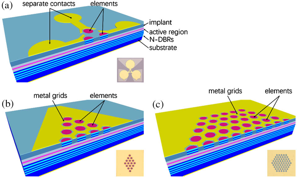
Fig. 1. (a) Structural diagram of three-element addressable array. The inset shows the top view of a fabricated three-element addressable array. (b) Cross-sectional sketch of a 16-element VCSEL array. The inset shows the top view of a fabricated 16-element array. (c) Cross-sectional sketch of a 61-element VCSEL array. The inset shows the top view of a fabricated 61-element array.
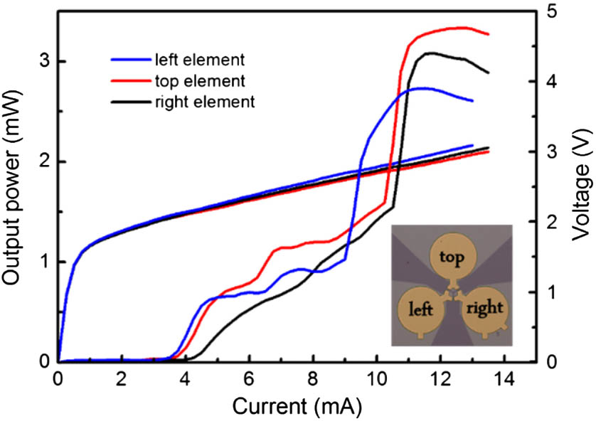
Fig. 2. Output power and voltage characteristics for injection currents supplied to the left element only, the top element only, and the right element only. The array elements are defined as the left element, the top element, and the right element, as shown in the inset.
Fig. 3. Near-field profiles of each element of the three-element array measured below and above the threshold.
Fig. 4. Schematic of experimental setup and positions used for measurement of the optical distribution, the near-field profiles, the far-field patterns, and the spectra to be measured.
Fig. 5. Top: optical field distributions in the active region of the array when measured for various I top I left I right
Fig. 6. Calculated index profiles through the left and top array elements (across the A A ′
Fig. 7. Output power of the array versus injection current I right I left I top
Fig. 8. (a) Top: measured near-fields of implant-defined 16-element in-phase coupled VCSEL arrays under various bias currents below threshold. Middle: measured near-fields of these arrays under various bias currents above threshold. Bottom: corresponding far-fields of these arrays measured at various currents above threshold. (b) P I
Fig. 9. Measured P I
Fig. 10. Measured P I
Fig. 11. Calculated current density (unit: A · m − 2

Set citation alerts for the article
Please enter your email address
© Copyright 2018-2021 | Chinese Laser Press. All Rights Reserved 沪ICP备15018463号-20