Abstract
Optical coupling behavior and associated effects in two-dimensional implant-defined coherently coupled vertical-cavity surface-emitting laser (VCSEL) arrays are studied via both experiments and theoretical calculations. Experiments show that optical coupling between array elements can enhance the array’s output power. Additionally, optical coupling via leaky optical fields can provide extra optical gain for the array elements, which can then reduce the thresholds of these elements. Elements can even be pumped without current injection to emit light by receiving a strong leaky optical field from other array elements. Optical coupling can also cause unusual phenomena: the central elements in large-area coherently coupled VCSEL arrays that lase prior to the outer elements when the arrays are biased, or the average injection current required for each element to lase, which is much lower than the threshold for a single VCSEL. Theoretical calculations are performed to explain the experimental results.1. INTRODUCTION
Physical interactions between multiple photonic oscillators can produce numerous unique properties that can be used in many different applications. One simple example is the optical coupling that occurs between multiple vertical-cavity surface-emitting lasers (VCSELs). When two or more VCSELs are optically coupled with each other, a coherently coupled VCSEL array is formed that allows radiation with a near-diffraction-limit beamwidth and high brightness to be obtained from the array [1]; this makes this type of array a viable candidate for fiber coupling and optical pumping applications. Additionally, when the VCSEL elements in the array are optically coupled, a fixed phase relationship is formed between the elements. By adjusting the phase relationship between the elements through wavelength detuning, beam steering can then be achieved [2–4]; this is useful in laser radar and laser printing. In addition, when optical coupling occurs between the array elements, the VCSEL array’s modulation bandwidth can also be greatly improved [5], and this has potential for application in optical communications. Therefore, optical coupling between the elements of coherently coupled VCSEL arrays is of major significance.
In general, optical coupling between VCSEL array elements can be realized using array structures containing narrow air gaps [6], reflectivity-modulation structures [7], phase-shifting layers [8], and regrown anti-guided array structures [1,9,10]. Among these approaches, the anti-guided array structure can achieve both stable in-phase and out-of-phase coupling by varying the inter-element spacing due to the leaky wave provided by the anti-guiding, while the other array structures can only achieve the less desirable out-of-phase coupling [1,9,10]. However, anti-guided array structures require extremely precise fabrication processes, including multi-step growth and high-fidelity anisotropic etching.
Proton implantation technology provides a much simpler and cheaper way to achieve optical coupling between VCSEL array elements [11–14]. The resulting implant-defined VCSEL arrays can also operate in both in-phase and out-of-phase coupling by varying the inter-element spacing because anti-guiding behavior can also be realized in these implanted arrays [15]. When compared with regrowth of the anti-guided structures, this method only requires fabrication of a proton implantation mask. (two elements) and (four elements) in-phase coherently coupled VCSEL arrays based on proton implantation were first reported by Choquette et al. [11]. We later realized two-dimensional (2D) in-phase coherently coupled arrays with high beam quality [12], and seven-element arrays with wide working ranges [13] based on proton implantation technology. Using metal grid electrodes, we then scaled the in-phase coherently coupled VCSEL arrays up in size from to (i.e., 100 elements) [14]. However, most previous research (including that on arrays fabricated via the other methods mentioned earlier) mainly focused on the beam quality of these arrays, while the optical coupling behavior between the elements and the associated effects on array performance were often ignored, particularly in arrays on scales that were larger than ; this is not advantageous for fabrication of large-size arrays.
Sign up for Photonics Research TOC. Get the latest issue of Photonics Research delivered right to you!Sign up now
In this work, 2D small-area three-element addressable coherently coupled VCSEL arrays and large-area 16-element and 61-element coherently coupled arrays are fabricated using the proton implantation technology. Measurements of the near-fields, far-fields, and emission spectra of these arrays are used to identify their lasing modes. The optical coupling behavior in the active regions of the three-element arrays under various bias conditions are monitored, and the accompanying phenomena that are associated with the optical coupling are analyzed theoretically. Experiments show that optical coupling between the elements not only increases array output power, but also reduces the thresholds of the array elements. Additionally, it is found that one element in the three-element coherently coupled array can be pumped to emit light using the strong leaky optical fields from the other two elements, even without bias current application, which proves the existence of the leaky waves in the proton implant-defined arrays experimentally. In addition, switching between the in-phase coupling and the out-of-phase coupling is realized by adjusting the injection currents of each element individually. Furthermore, optical coupling in these large-area coherently coupled VCSEL arrays can cause the central elements to lase prior to the outer elements and also reduces the currents that the array elements require to lase, which must be taken into account when designing large-size arrays.
2. DEVICE DESIGN AND FABRICATION
To investigate the optical coupling behavior of VCSEL arrays of different sizes, small-area three-element arrays and large-area 16-element and 61-element arrays were all designed. All these arrays were designed and fabricated using the same VCSEL wafer. Structural diagrams of the three-element, 16-element and 61-element arrays are shown in Figs. 1(a)–1(c), respectively. The VCSEL epitaxial material includes 34.5 pairs of N-type distributed Bragg reflector (DBR) mirrors and 22.5 pairs of P-type DBR mirrors grown on an N-type GaAs substrate that consists of alternating layers and three – quantum wells that are designed for a peak wavelength of 850 nm. All the array elements are defined by proton implantation and are designed to be circles with a diameter of 6 μm. The inter-element spacing for both the three-element and 16-element arrays is designed to be 4 μm. Because the lasing modes of the arrays are strongly dependent on the inter-element spacing [16], two different inter-element spacings of 4 μm and 6 μm are used in the 61-element arrays to study the optical coupling behavior in these arrays with the different lasing modes.
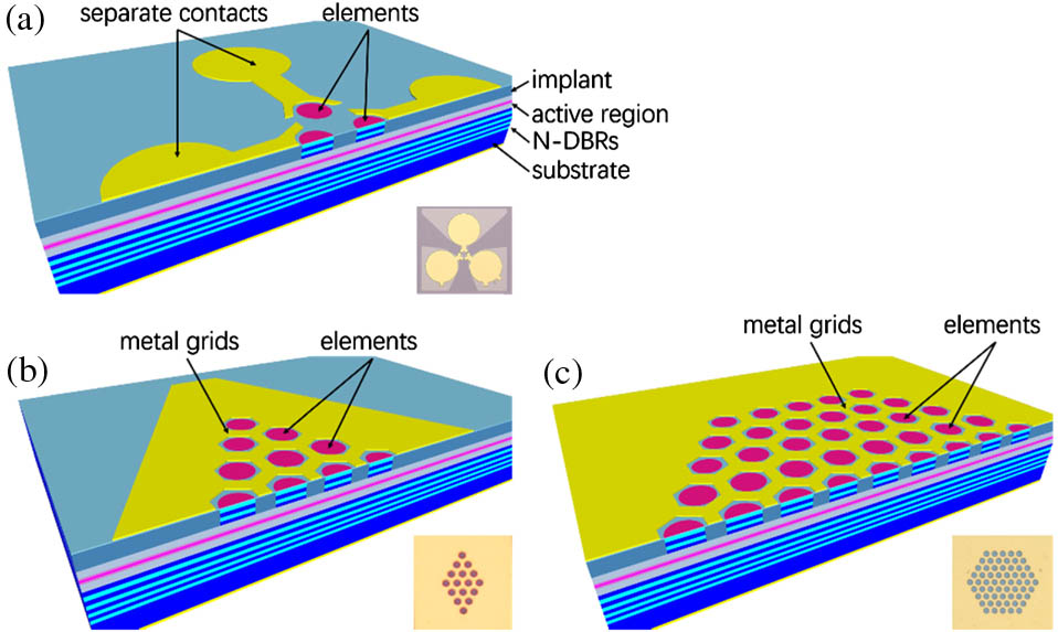
Figure 1.(a) Structural diagram of three-element addressable array. The inset shows the top view of a fabricated three-element addressable array. (b) Cross-sectional sketch of a 16-element VCSEL array. The inset shows the top view of a fabricated 16-element array. (c) Cross-sectional sketch of a 61-element VCSEL array. The inset shows the top view of a fabricated 61-element array.
The fabrication process used for the three-element arrays is as follows. First, a 3.5-μm-thick layer is formed on the surface of the cleaned VCSEL epitaxial wafer by plasma-enhanced chemical vapor deposition, and the that is deposited outside the emitting apertures (elements) is then etched away by a depth of 3 μm using an inductively-coupled plasma (ICP) process to form the proton implantation mask. The 0.5-μm-thick film that is left on the inter-element region protects the wafer from mechanical damage and also controls the implantation depth. Next, proton implantation is performed twice to achieve effective electrical isolation between the array elements. The implantation dose is fixed at , and the implantation energies of the two steps are 250 keV and 315 keV, respectively. After implantation, the mask is removed via wet etching. Next, separate Ti/Au top electrode layers with thicknesses of 15 nm and 300 nm, respectively, are formed via sputtering and a lift-off process. The substrate is then thinned to approximately 90 μm, and an AuGeNi/Au structure with layer thicknesses of 15 nm and 300 nm, respectively, is sputtered over the entire backside of the wafer to serve as the bottom electrode. Finally, rapid annealing is performed at 320°C for 35 s to form a good ohmic contact. The inset in Fig. 1(a) shows the top view of a fabricated three-element VCSEL array with separate contacts.
Figures 1(b) and 1(c) show schematic representations of the large-area implant-defined 16-element and 61-element VCSEL arrays, respectively. The insets show top views of the fabricated devices. Metal grids are used as top electrodes for these large-area arrays to provide uniform current injection. The fabrication process used for these large-area arrays is the same as that used for the three-element arrays. Note that the thickness of the layer that remains on the inter-element region after the ICP etching process to control the implantation depth is 0.8 μm, which ensures effective optical coupling in these arrays with their metal grid electrodes [14].
3. RESULTS AND DISCUSSION
A. Optical Coupling Behavior in Three-Element VCSEL Arrays
The separate contacts mean that the light–current–voltage (––) curves for each element in the three-element VCSEL arrays can be measured independently. Figure 2 shows the –– characteristics of each element in a typical three-element array under continuous wave conditions when measured at room temperature. The array elements are defined as the left element, the top element, and the right element, as shown in the inset. As the –– curves indicate, the threshold, the series resistance, and the output power of each element all differ from each other because of imperfections in the fabrication process. The threshold currents of the left element, the top element, and the right element are 3.5 mA, 3.7 mA, and 4.2 mA, respectively. Because the proton implantation provides only electrical confinement and no optical confinement in the array structure, the lasing mode of the array elements is unstable [17], and thus the output powers increase nonuniformly. The abrupt transitions shown in the –– curves indicate the onset of higher-order modes. Use of photonic crystals in the array may improve mode stability [17].

Figure 2.Output power and voltage characteristics for injection currents supplied to the left element only, the top element only, and the right element only. The array elements are defined as the left element, the top element, and the right element, as shown in the inset.
The near-field profiles of each element of the array below and above the threshold were obtained using a camera (Olympus DP 25, as shown in Fig. 4) and are shown in Fig. 3. The figure shows that, regardless of whether the injection current is below or above the threshold, only elements with current injection emit light, thus indicating that there is good electrical isolation between the array elements. The measured resistance values between contacts reach 6.0 MΩ, which makes it possible to control the injection current into each element independently.
Figure 3.Near-field profiles of each element of the three-element array measured below and above the threshold.
Figure 4.Schematic of experimental setup and positions used for measurement of the optical distribution, the near-field profiles, the far-field patterns, and the spectra to be measured.
The good electrical isolation between elements allows the injection current for each element to be controlled independently. Next, the optical coupling behavior between the elements in the active region under various bias conditions is monitored using a charge-coupled device (CCD) camera with a microscope objective that is connected to a laser beam profiler analysis system (Spiricon SP620 beam profiler). The focus of the CCD camera is adjusted along the optical axis to focus on the active region of the array. When the detected optical intensity reaches a maximum during focus adjustment, the camera is focused on the active region of the array, which then allows the optical field distribution in the active region to be obtained. Replacement of the microscope objective of the CCD camera with a closed-circuit television (CCTV) lens allows the far-field patterns of the array to be obtained. The emission spectra of the array are measured using an AQ6370 optical spectrum analyzer. The positions used for measurement of the optical distribution, the near-field profiles, the far-field patterns, and the spectra, along with the experiment setup, are shown in Fig. 4. Three current sources are used to drive each array element independently. The injection currents for the left element and the right element here were fixed at 3.8 mA (above the threshold of 3.5 mA) and 0 mA, respectively, and the injection current of the top element was then gradually increased from 0 mA to 3.8 mA. All measurements were taken under continuous wave conditions at room temperature. The measured optical field distributions in the active region, the far-field patterns, and the emission spectra acquired under various bias conditions are shown in Fig. 5.
Figure 5.Top: optical field distributions in the active region of the array when measured for various values while and were fixed at 3.8 mA and 0 mA, respectively. Bottom: spectra and far-field patterns measured under various bias conditions.
The optical field distributions in the top part of Fig. 5 show that when the injection current of the top element was 0 mA (i.e., ), no optical field was located within the top element, while the left element showed an unsaturated intensity. When was increased from 0 mA to 1.5 mA, the top element still did not lase, and its optical intensity was much weaker than that of the left element. However, an obvious saturated spot was found within the optical field of the left element, indicating that the optical intensity of the left element was enhanced. We believe that the anti-guiding in the array allowed the optical field of the left element to leak outward and be received by the top element as increased; the optical field of the top element could also leak outward and be received by the left element, meaning that the optical intensity of the left element increased. When increased to 2.0 mA, the top element then began to lase. Note that the threshold of the top element is 3.7 mA, according to the –– curve shown in Fig. 2. We believe that this top element obtains extra optical gain by receiving the leaky field from the left element, which means that the actual current injection that was required to lase in this case was much lower than the element’s own threshold. When , there is no interference fringe between the elements in the optical field distribution, and the far-field of the array shows a near-Gaussian distribution. Additionally, the spectrum that was obtained under this condition shows two separate spectral peaks (one from each element), which corresponds to incoherent operation [18]. These results demonstrate that the two elements are not optically coupled under this condition, and the optical gain provided by the leaky field is thus relatively weak and leads to a relatively weak optical intensity at the array. When increased to 2.7 mA and 3.0 mA, an interference fringe appeared between the elements, an on-axis lobe was found in the far-field pattern, and the two separate spectral peaks then overlapped into a single peak, thus indicating that the two elements are in-phase coherently coupled with single-mode operation at this current [16]. Under these conditions, the detected optical intensities of the entire array are saturated, which indicates that the extra optical gain is significantly enhanced and that the optical intensities of the two elements are thus greatly increased. When increased further to 3.5 mA and 3.8 mA, the interference fringe between elements disappeared, indicating that mode switching was occurring. Because the increase in the injection current changed both the carrier density and the temperature in the array, the emission wavelength and index profiles of the array both varied, thus causing the mode switching. At 3.8 mA, the far-field pattern shows an on-axis minimum intensity, while the spectrum of the array shows a single peak, thus demonstrating fundamental out-of-phase coupling characteristics [19]. In these cases, the right element was pumped sufficiently to emit light by the leaky fields from the other two elements, even without an applied bias current, indicating that the optical gain that it obtained from the other two elements was strong enough to cause it to emit light without current injection, which is a new phenomenon in coherently coupled VCSEL arrays.
To explain these experimental results further, the index profiles across the array (consisting of the left element and the top element) were calculated under various bias conditions using COMSOL Multiphysics software. In these calculations, the combined effects of the temperature and the carriers on the refractive index of the array are taken into account. An increase in temperature leads to an increase in the index, while carrier injection causes suppression of the refractive index. In general, the change in refractive index that is caused by temperature is [15]. In contrast, the change in the index caused by the carrier concentration is [15]. When increases, both and increase. Because is fixed at 3.8 mA and the array elements are electrically well isolated, the carrier concentration in the left element remains constant at approximately [15], meaning that the index change in the left element caused by the carriers is constant and equal to .
The carrier concentration in the top element at 3.8 mA is assumed to be the same as that in the left element, and it also suppresses the refractive index by . In addition, the carrier concentration in the top element under various injection currents is assumed to be proportional to the corresponding current densities, which means that the suppression of the refractive index at these different injection currents can be calculated. It should be noted that this assumption will lead to certain errors in the calculations, but this is acceptable because the carriers have little influence on the refractive index of the inter-element region of the array. Detailed calculations of the refractive index distribution can be found in our previous work [16]. Figure 6 shows the calculated index profiles through both the left and top array elements (corresponding to the – direction shown in the inset) under various bias conditions. As the image shows, the index of the emitting aperture is smaller than that of the inter-element region as a result of the combined effect of the temperature and the carriers, thus forming the so-called anti-guided array [1,9,10,15], where optical coupling between the elements is achieved via leaky waves. As increases, the refractive index of the inter-element region also increases, which may then enhance the leaky field intensity. When increases to 3.8 mA, the index of the inter-element region reaches its maximum within this current range, which means that the leaky field is strong enough to pump the right element such that it emits light. As the injection current changes, the index profile is varied due to the variation of the carriers and temperature, so the inter-element region may be tuned from in-phase resonant coupling of the array elements to out-of-phase resonant coupling of these elements. This may explain why the array transits abruptly into the out-of-phase mode beyond 3.5 mA.
Figure 6.Calculated index profiles through the left and top array elements (across the – direction shown in the inset) under various bias conditions.
In the subsequent measurements, we fixed and at 3.8 mA and 2.7 mA, respectively, and then varied from 0 mA to 4.2 mA to measure the output power and near- and far-field profiles of the array. The measured nonlinear – curve of the array is shown in Fig. 7. Each peak and valley in the light output shown in Fig. 7 corresponds to the different levels of optical coupling between the elements in the array. The insets depict the near- and far-field profiles that were obtained under various bias conditions. When , an interference fringe appeared between the elements, while the far-field pattern showed an on-axis maximum intensity, thus indicating the onset of in-phase optical coupling among the elements. However, the interference fringes were indistinct, and the intensities of the right element and the central lobe in the far-field were relatively weak, which indicated that the optical coupling strength was weak, and thus the output power was low in this case. When increased to 2.4 mA, the interference fringes became very bright and very obvious in the near-field profile, while the array showed a symmetrical optical distribution with increased intensity and the optical intensity of the central lobe in the far-field reached a maximum; this indicated strong optical coupling among the elements, thereby showing that the output power reached a maximum under these conditions. In this case, the beamwidth of the central lobe in the far-field was 3.6°, which is much smaller than that of a single VCSEL with the same aperture. When was increased further to 3.1 mA, the interference fringes became dim, and the optical intensity of the central lobe in the far-field decreased, thus indicating that the coupling strength was weak and the output power was low. When increased further to 3.6 mA, higher-order modes appeared in the array that were noticeable in the near-field, and the intensity of the central lobe in the far-field was approximately equal to that of the left-side lobe. In this case, the intensities of the near-field and far-field profiles became stronger than that of the case where , and the output power subsequently increased. However, the coherent coupling with the higher-order mode shows lower output power than the coherent coupling with the fundamental mode. From these results, we conclude that strong optical coupling can enhance the output power of the array.
Figure 7.Output power of the array versus injection current when and were fixed at 3.8 mA and 3.2 mA, respectively. The insets show the near-field (NF) and far-field (FF) profiles that were measured at different currents for the right element.
B. Optical Coupling Behavior in Large-Area 16-Element and 61-Element VCSEL Arrays
The beamwidth of a coherently coupled VCSEL array is inversely proportional to the size of the entire array, and the radiation mode intensity increases with the square of the number of array elements [1]. Therefore, use of increased numbers of array elements can not only enhance the output power and brightness, but also achieve a narrow beamwidth. Therefore, large-area coherently coupled VCSEL arrays are highly desirable for many applications and have become a focus of research. Here, we characterize the large-area 16-element and 61-element arrays and discuss the optical coupling behavior of these arrays based on the optical coupling behavior observed in the small-area three-element arrays.
The – curve of a typical 16-element array that was measured at room temperature under continuous wave conditions is shown in Fig. 8(b). The measured threshold of this array is approximately 20 mA. Because of a lack of effective heat dissipation measures, the output power of this array is relatively low. Higher output powers can be achieved by improving the device’s heat dissipation. The far-field patterns of the array that were measured above the threshold, as shown in the bottom row of Fig. 8(a), show an on-axis maximum intensity where the central lobe is surrounded by six weaker lobes, thus indicating in-phase coupling between the elements. A single peak is found in each of the spectra measured at 20, 25, and 30 mA that are shown in Fig. 8(c), which indicates that all elements are in-phase coherently coupled with single-mode operation within this current range. All these results prove that in-phase coupling is achieved in this array. When the near-field profiles were measured under various bias conditions, an unusual phenomenon that the outer elements lase after the central elements was observed in almost all the coherently coupled 16-element VCSEL arrays. As indicated by the near-field profiles measured below threshold, which are shown on the top row of Fig. 8(a), when the injection current was 2 mA, the four central elements were emitting light, while the other elements were still dim. As the current increased from 2 mA to 15 mA, the array elements were gradually illuminated in order from the inside to the outside. When the current increased above the threshold, a similar phenomenon was observed in the array, as shown in the near-field profiles that were measured above threshold and in the middle row of Fig. 8(a). At 20 mA, the two elements that were located at the center of the array were lasing. As a result of imperfect fabrication processes, the elements on the bottom-right side may have lower thresholds that allow them to lase simultaneously with the two central elements at 20 mA. When the current increased to 25 mA, the elements that were located in the three central rows were then stimulated to lase, while the elements that were located on the very outside of the array still did not lase. When the current increased further to 30 mA, all the elements lased with uniform intensity, and the beamwidth of the central lobe in the far-field was 2.8°, which is smaller than that of the three-element array. In this case, the average injection current required for each element [mA/(number of elements)] to lase was approximately only 1.9 mA, which is much lower than that required for a single VCSEL.
Figure 8.(a) Top: measured near-fields of implant-defined 16-element in-phase coupled VCSEL arrays under various bias currents below threshold. Middle: measured near-fields of these arrays under various bias currents above threshold. Bottom: corresponding far-fields of these arrays measured at various currents above threshold. (b) – curve of 16-element VCSEL array under continuous wave conditions. (c) Spectra of the array measured under different current conditions.
Similar phenomena were also observed in the large-area 61-element coherently coupled VCSEL arrays. Figure 9 shows the – curve of a typical 61-element array with inter-element spacing of 4 μm. The threshold of this array was approximately 30 mA. The near-field profiles, far-field patterns, and spectra that were measured at different currents are shown in the insets. The optical energy is mainly concentrated in the central lobe in the far-fields, and a single peak was found in each of the spectra, indicating the array’s strong in-phase coupling characteristics. In this in-phase coherently coupled 61-element array, the phenomenon that the central elements of the array lased prior to the outer elements was also observed in the measured near-field profiles. When the injection current was 40 mA, the elements that were located at the array center were lasing, while the outer elements still did not lase. When the current was increased to approximately 47 mA, all elements were lasing with the exception of the elements located near the edge of the array. When the current increased further to approximately 57 mA, all elements in the array were then lasing, and the average injection current required for each element to lase was only 0.93 mA. In addition, the beamwidth of the array in this case was 2.3°, which is smaller than that of the 16-element array.
Figure 9.Measured – characteristics of a 61-element in-phase coupled VCSEL array. The insets shown on the right are the near-fields, far-fields, and spectra that were measured at different currents.
Figure 10 shows the near-field profiles, the far-field patterns, and the spectra of a 61-element array with 6-μm inter-element spacing at various currents. Unlike the far-field patterns of the in-phase coupled 61-element array, the far-field of this array shows an on-axis null, and the optical energy is divided into several lobes; in addition, a single peak was also found in each of the spectra measured under different conditions, thus indicating that the array was operating in the out-of-phase mode. The near-field profiles show that when the current was gradually increased, the elements that were located at the center of the array lased prior to the outer elements. Figure 10 shows that when the array injection current was 63 mA, all elements were lasing. At this point, the average injection current for the array elements was only 1.03 mA, which is much lower than the threshold of a single VCSEL.
Figure 10.Measured – characteristics of a 61-element out-of-phase coupled VCSEL array. The insets shown on the right are the near-fields, far-fields, and spectra that were measured at different currents.
These measured results show that the phenomena that the central elements lase prior to the outer elements and that the threshold for each element is dramatically reduced are found in in-phase coupled arrays of different sizes and are even found in both in-phase and out-of-phase coupled arrays. During the preparation of these large-area arrays, metal grid electrodes are used to ensure uniform current injection. The current density distribution above the threshold of each array was calculated using COMSOL Multiphysics software. These calculations excluded any nonuniformities among the elements. The calculated results presented in Fig. 11 show that the current density is uniform across the array because of the use of the metal grids. These calculated results indicate that all array elements would lase simultaneously at a uniform current density, but the experimental results are inconsistent with these theoretical calculations. The optical coupling between the elements is believed to cause these unusual phenomena in the large-area coherently coupled VCSEL arrays. As the discussion for the three-element arrays, the elements are optically coupled with each other through leaky waves, and thus the optical field of each element can leak outward and be received by the other elements. Because the central elements have the largest numbers of surrounding elements, they receive more leaky optical fields than the outer elements, and thus have greater optical gain and will lase first, even at a uniform current density. Because of the optical coupling between the elements, these elements obtain extra optical gain, which means that the average injection current required for each element to lase is much lower than that required for a single VCSEL.
Figure 11.Calculated current density (unit: ) distribution of 61-element VCSEL array with metal grids.
These phenomena and results indicate that when large-scale coherently coupled arrays are prepared, the aperture sizes of the central elements should be increased appropriately to counteract the optical gain that is obtained from optical coupling among the elements to achieve a uniform optical intensity across the elements; this would allow the beam quality of the array to be further enhanced [20].
4. CONCLUSIONS
Optical coupling behavior in coherently coupled VCSEL arrays has been studied. Experiments showed that optical coupling between the array elements not only reduces the lasing thresholds of the array elements, but also enhances the output powers of these arrays. In addition, optical coupling in large-area coherently coupled VCSEL arrays can cause the central elements to lase prior to the outer elements and can also reduce the average injection current required for the array elements to lase. Study of the optical coupling behavior can provide a deeper understanding of the coupling mechanisms of these arrays, and it can also guide us in the design and fabrication of larger-size arrays with higher performance.
References
[1] L. Bao, N.-H. Kim, L. J. Mawst, N. N. Elkin, V. N. Troshchieva, D. V. Vysotsky, A. P. Napartovich. Near-diffraction-limited coherent emission from large aperture antiguided vertical-cavity surface-emitting laser arrays. Appl. Phys. Lett., 84, 320-322(2004).
[2] D. F. Siriani, K. D. Choquette. Electronically controlled two-dimensional steering of in-phase coherently coupled vertical-cavity laser arrays. IEEE Photon. Technol. Lett., 23, 167-169(2011).
[3] M. Xun, C. Xu, Y. Xie, G. Jiang, G. Pan, Y. Dong, H. Chen. Beam steering in highly coherent implant-defined vertical cavity surface emitting laser array. CLEO (2016)(2016).
[4] M. J. Adams, N. Li, B. R. Cemlyn, H. Susanto, I. D. Henning. Effects of detuning, gain-guiding, and index antiguiding on the dynamics of two laterally coupled semiconductor lasers. Phys. Rev. A, 95, 053869(2017).
[5] S. T. M. Fryslie, Z. Gao, H. Dave, B. J. Thompson, K. Lakomy, S. Lin, P. J. Decker, D. K. McElfresh, J. E. Schutt-Aine, K. D. Choquette. Modulation of coherently coupled phased photonic crystal vertical cavity laser arrays. IEEE J. Sel. Top. Quantum Electron., 23, 1700409(2017).
[6] H. Yoo, A. Scherer, J. P. Harbison, L. T. Florez, E. G. Paek, B. P. Van der Gaag, J. R. Hayes, A. Von Lehmen, E. Kapon, Y. Kwon. Fabrication of a two‐dimensional phased array of vertical‐cavity surface‐emitting lasers. Appl. Phys. Lett., 56, 1198-1200(1990).
[7] M. Orenstein, E. Kapon, N. G. Stoffel, J. P. Harbison, L. T. Florez, J. Wullert. Two-dimensional phase-locked arrays of vertical-cavity semiconductor lasers by mirror reflectivity modulation. Appl. Phys. Lett., 58, 804-806(1991).
[8] M. E. Warren, P. L. Gourley, G. R. Hadley, G. A. Vawter, T. M. Brennan, B. E. Hammons, K. L. Lear. On-axis far-field emission from two-dimensional phase-locked vertical cavity surface-emitting laser arrays with an integrated phase-corrector. Appl. Phys. Lett., 61, 1484-1486(1992).
[9] D. Zhou, L. J. Mawst, Z. Dai. Modal properties of two-dimensional antiguided vertical-cavity surface-emitting laser arrays. IEEE J. Quantum Electron., 38, 652-664(2002).
[10] L. Bao, N.-H. Kim, L. J. Mawst, N. N. Elkin, V. N. Troshchieva, D. V. Vysotsky, A. P. Napartovich. Modeling, fabrication, and characterization of large aperture two-dimensional antiguided vertical-cavity surface-emitting laser arrays. IEEE J. Sel. Top. Quantum Electron., 11, 968-981(2005).
[11] A. C. Lehman, K. D. Choquette. One- and two-dimensional coherently coupled implant-defined vertical-cavity laser arrays. IEEE Photon. Technol. Lett., 19, 1421-1423(2007).
[12] M.-M. Mao, C. Xu, Q. Kan, Y.-Y. Xie, M. Xun, K. Xu, J.-C. Liu, H.-Q. Ren, H.-D. Chen. High beam quality of in-phase coherent coupling 2-D VCSEL arrays based on proton-implantation. IEEE Photon. Technol. Lett., 26, 395-397(2014).
[13] M. Xun, C. Xu, J. Deng, Y. Xie, G. Jiang, J. Wang, K. Xu, H. Chen. Wide operation range in-phase coherently coupled vertical cavity surface emitting laser array based on proton implantation. Opt. Lett., 40, 2349-2352(2015).
[14] G. Pan, Y. Xie, C. Xu, M. Xun, Y. Dong, J. Deng, J. Sun. Large-scale proton-implant-defined VCSEL arrays with narrow beamwidth. IEEE Electron Device Lett., 39, 390-393(2018).
[15] D. F. Siriani, K. D. Choquette. Implant defined anti-guided vertical-cavity surface-emitting laser arrays. IEEE J. Quantum Electron., 47, 160-164(2011).
[16] M. Xun, C. Xu, Y. Y. Xie, J. Deng, K. Xu, H. D. Chen. Modal properties of 2-D implant-defined coherently coupled vertical-cavity surface-emitting laser array. IEEE J. Quantum Electron., 51, 2600106(2015).
[17] D. F. Siriani, K. D. Choquette. In-phase, coherent photonic crystal vertical-cavity surface-emitting laser arrays with low divergence. Electron. Lett., 46, 712-714(2010).
[18] M. T. Johnson, D. F. Siriani, M. P. Tan, K. D. Choquette. High-speed beam steering with phased vertical cavity laser arrays. IEEE J. Sel. Top. Quantum Electron., 19, 1701006(2013).
[19] M. T. Johnson, D. F. Siriani, J. D. Sulkin, K. D. Choquette. Phase and coherence extraction from a phased vertical cavity laser array. Appl. Phys. Lett., 101, 031116(2012).
[20] G. Pan, Y. Xie, C. Xu, M. Xun, Y. Dong, J. Deng, H. Chen, J. Sun. Dependence of beam quality on optical intensity asymmetry in in-phase coherently coupled VCSEL array. IEEE J. Quantum Electron., 54, 2400306(2018).


