• Photonics Research
  • Vol. 8, Issue 3, 257 (2020)
Jinman Lv1, Binbin Hong1, Yang Tan2, Feng Chen2, Javier Rodríguez Vázquez de Aldana3, and Guo Ping Wang1、*
Author Affiliations
  • 1Institute of Microscale Optoelectronics, Shenzhen University, Shenzhen 518052, China
  • 2School of Physics, State Key Laboratory of Crystal Materials, Shandong University, Jinan 250100, China
  • 3Departamento Física Aplicada, Facultad Ciencias, Universidad de Salamanca, Salamanca 37008, Spain
  • show less
    DOI: 10.1364/PRJ.380215 Cite this Article Set citation alerts
    Jinman Lv, Binbin Hong, Yang Tan, Feng Chen, Javier Rodríguez Vázquez de Aldana, Guo Ping Wang. Mid-infrared waveguiding in three-dimensional microstructured optical waveguides fabricated by femtosecond-laser writing and phosphoric acid etching[J]. Photonics Research, 2020, 8(3): 257 Copy Citation Text show less
    Schematic processes of (a) fs-laser inscription and (b) H3PO4 acid etching for the microstructured optical waveguide in YAG crystal. The insets are the images of the two processes.
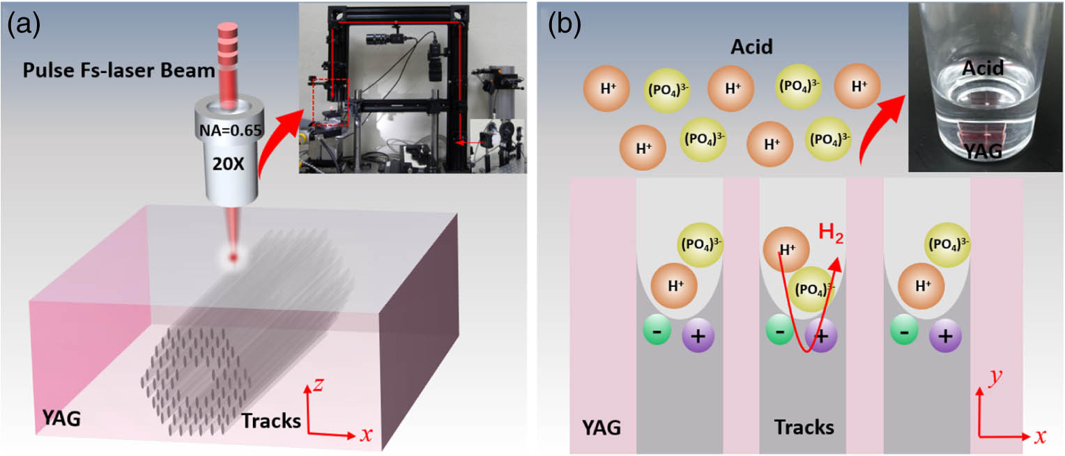
    Fig. 1. Schematic processes of (a) fs-laser inscription and (b) H3PO4 acid etching for the microstructured optical waveguide in YAG crystal. The insets are the images of the two processes.
    (a) Microscopic images of the end-faces and top-view patterns at the etching time of 0, 3, 30, and 60 h and (b) the etched dimensions of microchannel depth as a function of the etching time.
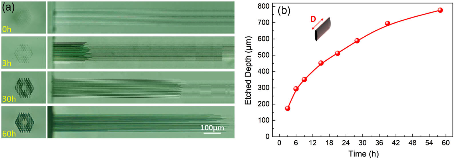
    Fig. 2. (a) Microscopic images of the end-faces and top-view patterns at the etching time of 0, 3, 30, and 60 h and (b) the etched dimensions of microchannel depth as a function of the etching time.
    (a) Etched dimensions of microchannel width and length as a function of the etching time. (b) The schematic illustration of a tapered X-shaped microchannel formed inside YAG crystal at the lasing wavelength of ∼1064 nm. The microscopic images of the cross section (c) before polished and (d) after polished.
    Fig. 3. (a) Etched dimensions of microchannel width and length as a function of the etching time. (b) The schematic illustration of a tapered X-shaped microchannel formed inside YAG crystal at the lasing wavelength of 1064  nm. The microscopic images of the cross section (c) before polished and (d) after polished.
    (a) Calculated transmission spectrum for MOW; simulated intensity profiles (b) at 632.8 nm, (c) at 1550 nm, (d) at 4000 nm; and (e) simulated intensity profile at 4000 nm for waveguide not etched.
    Fig. 4. (a) Calculated transmission spectrum for MOW; simulated intensity profiles (b) at 632.8 nm, (c) at 1550 nm, (d) at 4000 nm; and (e) simulated intensity profile at 4000 nm for waveguide not etched.
    Dispersion curves and mode structures of the proposed fiber. (a) Dispersion curves. The red line corresponds to the guided HE11 mode and the blue solid lines are the bands for cladding modes. The black circle represents the COMSOL simulation result at 4 μm. (b) The y component of electric field (Ey) at 4 μm obtained from MPB. The field increases from white to red. Periodic boundaries are applied. (c) Ey at 4 μm obtained from COMSOL. The field increases from blue to red. A perfectly matched layer is applied at the thin outmost layer of the structure.
    Fig. 5. Dispersion curves and mode structures of the proposed fiber. (a) Dispersion curves. The red line corresponds to the guided HE11 mode and the blue solid lines are the bands for cladding modes. The black circle represents the COMSOL simulation result at 4 μm. (b) The y component of electric field (Ey) at 4 μm obtained from MPB. The field increases from white to red. Periodic boundaries are applied. (c) Ey at 4 μm obtained from COMSOL. The field increases from blue to red. A perfectly matched layer is applied at the thin outmost layer of the structure.
    Measured near-field modal profiles along (a) HE11(1) and (b) HE11(2) polarization at 4 μm. (c) The polar image of propagation losses of MOW at 4 μm.
    Fig. 6. Measured near-field modal profiles along (a) HE11(1) and (b) HE11(2) polarization at 4 μm. (c) The polar image of propagation losses of MOW at 4 μm.
    Jinman Lv, Binbin Hong, Yang Tan, Feng Chen, Javier Rodríguez Vázquez de Aldana, Guo Ping Wang. Mid-infrared waveguiding in three-dimensional microstructured optical waveguides fabricated by femtosecond-laser writing and phosphoric acid etching[J]. Photonics Research, 2020, 8(3): 257
    Download Citation