We fabricated a three-dimensional microstructured optical waveguide (MOW) in a single-crystal using the femtosecond-laser writing and phosphoric acid etching techniques, and observed excellent midinfrared waveguiding performance with low loss of ~. Tracks with a periodic arrangement were written inside the yttrium aluminum garnet (YAG) crystal via femtosecond laser inscription, and then etched by the phosphoric acid () to form the hollow structures. The evolution of the microstructure of tracks was investigated in detail. The function of the MOW was analyzed by different numerical methods, indicating the proposed MOW can effectively operate in quasi-single-mode pattern in the midinfrared wavelength range, which agrees well with our experiment results.
1. INTRODUCTION
As the basic components in integrated photonics, microstructured optical waveguides (MOWs) can confine the cross sections of propagating light on the micron scale, thus achieving higher local optical intensities compared with the bulk materials [1]. MOW devices including the demultiplexers, routers, switches, and modulators have been widely used in optical telecommunication systems [2]. Recently, great attention has been paid to the midinfrared wavelength regime due to its strong absorption properties for various gases and molecules, which enables midinfrared MOW devices applied in various fields, such as environmental monitoring, trace gas detecting, biochemical sensing, and free-space optical communication [3–5].
Efforts on the fabrication of MOW devices have been predominantly focused on ion/proton exchange, metal-ion diffusion, and ion implantation/irradiation in a wide range of optical materials [6–10]. Nevertheless, these traditional technologies are difficult for three-dimensional (3D) micronano optical waveguides fabrication because they generally suffer from the complicated processes and hence inefficiency for complex geometries. Recently, the advent of the femtosecond laser (fs-laser) writing offers a powerful solution to this dilemma [11–14]. Particularly, it has wide applicability of materials and has the advantages of rapid and maskless 3D processing ability and negligible thermal-diffusion effect [15]. In addition, a combined approach of material modification followed by chemical etching provides the possibility to manufacture 3D microchannels for integrated optical or microfluidic devices [16–21]. Combining the laser writing with the wet etching, Ródenas et al. [18] recently reported the fabrication of subwavelength diffraction gratings and nanostructured optical waveguides in yttrium aluminum garnet (YAG) and millimeter-long nanopores in sapphire. In this hybrid technique, the process of material modification by fs-laser is utilized for changing the refractive index and chemical stability of the patterns for forming the photonic structures after acid etching. In previous work, structures of rod array with high aspect ratio on quartz glass and slide glass have been fabricated successfully by controlling two-step etchings with the high etching selectivity between intrinsic material and modified area [22,23].
Optical crystals are important materials for many optical devices [24–26]. For instance, electrooptic crystals could be used in the domain of light phase, energy, and polarization. Nonlinear crystals could be utilized for frequency converters of light. Besides, laser crystals could be applied as gain media in solid-state laser systems with lower lasing thresholds than glasses. Particularly, the YAG crystal is a multifunctional platform for numerous optical applications [27].
Sign up for Photonics Research TOC. Get the latest issue of Photonics Research delivered right to you!Sign up now
In this work, we report the fabrication of the MOW in YAG crystal via fs-laser inscription combining with the etching process and realization of excellent midinfrared waveguiding performance with low loss of . The relationship of the etching condition and the etching rate was investigated. The optical transmittance in the MOW versus the wavelength was calculated by the transmission matrix method. Based on the calculation results, the light propagation in the MOW for the midinfrared band was investigated both numerically and experimentally.
2. EXPERIMENTAL DETAILS
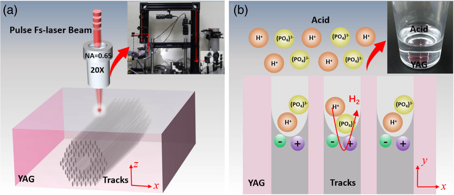
The YAG crystal, used in this work, was cut into dimensions of and optically polished. The MOW was fabricated following three steps. First, the 3D photonic-crystal-like pattern was written inside the YAG crystal by the ultrafast laser writing method along the axis. The influence of the laser inscription parameters on the corrosion behavior was discussed by Hasse et al. [21]. According to their work and combining with our certain equipment, we adjusted our laser inscription parameters accordingly. During the microstructuring process, an amplified Ti:sapphire femtosecond laser (Spitfire, Spectra Physics) was utilized to deliver linearly polarized pulsed laser (pulse duration of 120 fs, central wavelength of 795 nm, and repetition rate of 1 kHz). The beam is focused by a microscope objective () and the average power is reduced to 1.2 mW. The sample is placed on an motorized stage that allows the sample scanned at a constant speed (500 μm/s) and irradiated by laser at a point about 150 μm beneath the surface of . Parallel scans of a sample are done to obtain the required 3D photonic-crystal-like pattern. Figure 1(a) illustrates schematically the fabrication procedure for the YAG photonic-crystal-like structures, and the image of the fs-laser inscription system is shown in the inset of Fig. 1(a). Second, the sample was immersed in a 50% aqueous solution of acid for 180 h in an ultrasonic bath at room temperature, as shown in Fig. 1(b) and the inset. At last, the facets of the sample were optically polished to dimensions of . The microstructure of the YAG MOW was imaged by the optical microscope (Axio Imager, Carl Zeiss), before and after the etching.
Figure 1.Schematic processes of (a) fs-laser inscription and (b) acid etching for the microstructured optical waveguide in YAG crystal. The insets are the images of the two processes.
Figure 2(a) presents microscopic images of the end-faces and top-view patterns with the etching time of 0, 3, 30, and 60 h, respectively. Before the etching, the fs-laser inscribed area is much brighter showing clear parallel lines. During the etching, the inscribed line patterns dissolved, and the appearance of the lines turned from bright to dark near the end-facet of the crystal. Along the etching time, the dark line got longer and longer. Figure 2(b) shows the depth (D) of the etched lines along with the etching time. Please note, the etching rate was decreased with the extending of the etched microchannel. The concentration of acid is decreased inside the YAG crystal, due to the chemical reaction of and the inscribed crystal.
Figure 2.(a) Microscopic images of the end-faces and top-view patterns at the etching time of 0, 3, 30, and 60 h and (b) the etched dimensions of microchannel depth as a function of the etching time.
Figure 3(a) displays the variation of the width (W)/length (L) of the cross section of the track. We see that as time grows, the etched W is increased gradually, while the etched L almost remains a constant. In previous investigations, researchers usually focused their study on how the fs-laser parameters influence the corrosion of the longitudinal depth [21,23], while leaving the corrosion process of the cross section of tracks not investigated. In this work, we found that there is a difference between the corrosion behaviors of the width and length. Based on the measured etching processes in Fig. 3(a), we calculated the shape of the etched tracks after the etching time of 180 h. As shown in Fig. 3(b), there are two tapered microchannels with a depth of 0.4 mm near the surface of the YAG crystal. To fabricate the MOW, we cut the tapered channel off after the acid etching and repolished the cutting facet. Figures 3(c) and 3(d) show images of the cross section before and after the polishing.
Figure 3.(a) Etched dimensions of microchannel width and length as a function of the etching time. (b) The schematic illustration of a tapered X-shaped microchannel formed inside YAG crystal at the lasing wavelength of . The microscopic images of the cross section (c) before polished and (d) after polished.
We calculated the transmission of the light in the center of the etched MOW, according to the transmission matrix method following the equation below [28]: where is the vacuum wavelength, is the frequency of the incident wave, , , , and are the matrix elements for the whole transfer matrix, and is the refractive index of the substrate [29].
Figure 4(a) shows the calculated transmission as a function of wavelength; it also shows the transmission increases along with the wavelength. And the light can be better confined in the etched MOW within the midinfrared range. To further prove it, the propagation mode of the MOW was calculated by the finite-difference beam propagation method (FD-BPM) [30]. Figures 4(b)–4(d) show the propagation of the light with the wavelength of 632.8, 1550, and 4000 nm, respectively. As easily seen, the midinfrared light is well confined in the etched MOW, which indicates the etched MOW can be used as the quasi-single-mode midinfrared waveguide.
Figure 4.(a) Calculated transmission spectrum for MOW; simulated intensity profiles (b) at 632.8 nm, (c) at 1550 nm, (d) at 4000 nm; and (e) simulated intensity profile at 4000 nm for waveguide not etched.
To analyze the guiding mechanism of the microstructure, we calculated its dispersion curves using the MIT Photonic Bands (MPB) package [31] which is based on the plane wave expansion method. The dispersion curves of the fiber are shown in Fig. 5(a), which shows that the band for the fundamental mode lies in the gap between the bands for the cladding modes (blue solid lines) distributed in the bulky microstructured region and the light line (green dashed line), so the wave is confined in the central defect region via effective total-internal reflection. Figure 5(b) shows the mode structure of the fundamental mode at 4 μm calculated using MPB, which is double-confirmed by COMSOL simulation, shown in Fig. 5(c). The effective refractive indices of the eigenvalue obtained by MPB and COMSOL at the operating 4 μm wavelength are consistent with each other, shown in Fig. 5(a), which validates the simulation results.
Figure 5.Dispersion curves and mode structures of the proposed fiber. (a) Dispersion curves. The red line corresponds to the guided mode and the blue solid lines are the bands for cladding modes. The black circle represents the COMSOL simulation result at 4 μm. (b) The component of electric field () at 4 μm obtained from MPB. The field increases from white to red. Periodic boundaries are applied. (c) at 4 μm obtained from COMSOL. The field increases from blue to red. A perfectly matched layer is applied at the thin outmost layer of the structure.
We measured the propagation mode of the etched MOW at the wavelength of 4 μm. During the measurement, the midinfrared laser (MIRTM 8025, Daylight Solutions, Inc.) was coupled into the etched MOW by an end-face coupling arrangement [32]. As shown in Figs. 6(a) and 6(b), the MOW was supported by fundamental mode guiding at 4000 nm for both the and polarizations, respectively. It means the promising capability of fs-laser inscription combined with acid etching micromachining MOW in YAG crystal for MIR applications. To obtain thorough information on the polarization effects of the guidance, we measured the all-angle light transmission along the transverse plane [Fig. 6(c)]. It is found that the guidance is polarization-independent (i.e., the guidance exists for the input light at any transverse polarizations). Although the tracks or the cross section of the hollow is extremely asymmetric (it is elliptical with very large aspect ratio), the light is not guided by the tracks but the region surrounded by the tracks which is rather symmetric on the plane (perpendicular to the light propagating direction), as shown in Fig. 1(a). This makes the light intensity profiles in the waveguide almost isotropic, see the numerical results in Figs. 4(b)–4(d) and experimental results in Figs. 6(a) and 6(b). Therefore, the system is almost isotropic on the plane, and the difference between the ( polarized) and ( polarized) polarizations is actually very small, revealing a perfect isotropic light confinement capability.
Figure 6.Measured near-field modal profiles along (a) and (b) polarization at 4 μm. (c) The polar image of propagation losses of MOW at 4 μm.
The total losses of the MOW (including propagation losses and coupling losses) were measured at 4 μm based on the end-face coupling system [32]. The coupling loss was estimated to be 0.7 dB by considering the overlap of the profiles of the incident light beam and waveguide modes. Details of estimating the propagation losses are found in Refs. [33,34]. Finally, the propagation loss of MOW was determined to be (according to the method proposed by Ref. [33], the systematic relative error for estimating the propagation loss is about 10%), showing an excellent light transmission property, which was better than the normal YAG not etched optical-lattice-like waveguide () fabricated only by fs-laser inscription [35]. The stronger light confinement can benefit the applications in integrated photonic devices based on compact structures. In addition, the higher light intensities are useful in diverse applications, such as lasing and nonlinear response. Additionally, for our etched MOW, the best confinement and nearly total transmission of light are located at the midinfrared wavelength regime, which is clearly seen from Figs. 4(a)–4(d). However, if the MOW is not etched, the best operation wavelength will be shifted to the nearinfrared wavelength regime, as reported in Ref. [35]. The propagation mode of the not etched MOW was also calculated by the finite-difference beam propagation method at 4 μm, as shown in Fig. 4(e). By comparing Figs. 4(d) and 4(e), our etched MOW works as a much better midinfrared MOW compared with the not etched one. Therefore, the superiority of the MOW is the restriction of the high intensity of the light in midinfrared wavelength range, which gives us a hint for the design of the novel waveguide for integrated optics.
4. CONCLUSION
We have fabricated a 3D hexagonal MOW in YAG crystal by fs-laser inscription combining with acid etching techniques. We have investigated the corrosion behaviors for different geometrical parameters of the tracks. The guiding properties have been numerically investigated by multiple methods, and verified in experiments. The measured near-field modal profiles of MOW exhibit an excellent midinfrared waveguiding performance with low loss of . This work suggests that this hybrid technique which combines the laser inscription with the acid etching could be an efficient method to fabricate diverse photonic devices for various wavelength regimes.
Acknowledgment
Acknowledgment. We thank Dr. Neng Wang for constructive discussions and Zhen Shang for some help in experiments.
[28] J. Tang, H. J. Yang, Q. Xu, J. W. Liao, S. Yuan, Y. Hu. Analysis of the transfer characteristics of one-dimensional photonic crystal and its application with transfer matrix method. Infrared Laser Eng., 39, 76-80(2010).