• Acta Physica Sinica
  • Vol. 68, Issue 24, 247203-1 (2019)
Yan-Li Liu1, Wei Wang1, Yan Dong2, Dun-Jun Chen2、*, Rong Zhang2, and You-Dou Zheng2
Author Affiliations
  • 1School of Information and Electronic Engineering, Shandong Technology and Business University, Yantai 264005, China
  • 2School of Electronic Science and Engineering, Nanjing University, Nanjing 210093, China
  • show less
    DOI: 10.7498/aps.68.20191153 Cite this Article
    Yan-Li Liu, Wei Wang, Yan Dong, Dun-Jun Chen, Rong Zhang, You-Dou Zheng. Effect of structure parameters on performance of N-polar GaN/InAlN high electron mobility transistor[J]. Acta Physica Sinica, 2019, 68(24): 247203-1 Copy Citation Text show less

    Abstract

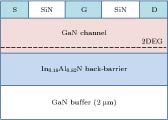
    Based on the drift-diffusion transport model, Fermi-Dirac statistics and Shockley-Read-Hall recombination model, the effect of the structure parameters on the performance of N-polar GaN/InAlN high electron mobility transistor is investigated by self-consistently solving the Schrodinger equation, Poisson equation and carrier continuity equation. The results indicate that the saturation current density of the device increases and the threshold voltage shifts negatively with GaN channel thickness increasing from 5 nm to 15 nm and InAlN back barrier thickness increasing from 10 nm to 40 nm. The maximum transconductance decreases with GaN channel thickness increasing or InAlN back barrier thickness decreasing. The change trends of the various performance parameters become slow gradually with the increase of the thickness of the GaN channel layer and InAlN back barrier layer. When the GaN channel thickness is beyond 15 nm or the InAlN back barrier thickness is more than 40 nm, the saturation current, the threshold voltage and the maximum transconductance tend to be stable. The influence of the structure parameter on the device performance can be mainly attributed to the dependence of the built-in electric field, energy band structure and the two-dimensional electron gas (2DEG) on the thickness of the GaN channel layer and InAlN back barrier layer. The main physical mechanism is explained as follows. As the GaN channel thickness increases from 5 nm to 15 nm, the bending of the energy band in the GaN channel layer is mitigated, which means that the total built-in electric field in this layer decreases. However, the potential energy drop across this GaN channel layer increases, resulting in the fact that the quantum well at the GaN/InAlN interface becomes deeper. So the 2DEG density increases with GaN channel thickness increasing. Furthermore, the saturation current density of the device increases and the threshold voltage shifts negatively. Moreover, due to the larger distance between the gate and the 2DEG channel, the capability of the gate control of the high electron mobility transistor decreases. Similarly, the depth of the GaN/InAlN quantum well increases with InAlN back barrier thickness increasing from 10 nm to 40 nm, which results in the increase of the 2DEG concentration. Meanwhile, the electron confinement in the quantum well is enhanced. Therefore the device saturation current and the maximum transconductance increase with InAlN back barrier thickness increasing.
    Yan-Li Liu, Wei Wang, Yan Dong, Dun-Jun Chen, Rong Zhang, You-Dou Zheng. Effect of structure parameters on performance of N-polar GaN/InAlN high electron mobility transistor[J]. Acta Physica Sinica, 2019, 68(24): 247203-1
    Download Citation