• Acta Physica Sinica
  • Vol. 68, Issue 24, 247203-1 (2019)
Yan-Li Liu1, Wei Wang1, Yan Dong2, Dun-Jun Chen2、*, Rong Zhang2, and You-Dou Zheng2
Author Affiliations
  • 1School of Information and Electronic Engineering, Shandong Technology and Business University, Yantai 264005, China
  • 2School of Electronic Science and Engineering, Nanjing University, Nanjing 210093, China
  • show less
    DOI: 10.7498/aps.68.20191153 Cite this Article
    Yan-Li Liu, Wei Wang, Yan Dong, Dun-Jun Chen, Rong Zhang, You-Dou Zheng. Effect of structure parameters on performance of N-polar GaN/InAlN high electron mobility transistor[J]. Acta Physica Sinica, 2019, 68(24): 247203-1 Copy Citation Text show less
    Schematic of N-polar GaN/InAlN HEMT structure.N极性面GaN/InAlN HEMT结构示意图
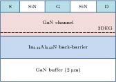
    Fig. 1. Schematic of N-polar GaN/InAlN HEMT structure.N极性面GaN/InAlN HEMT结构示意图
    (a) Output characteristics, (b) transfer characteristics, and (c) transconductance curves of N-polar GaN/InAlN HEMTs with different GaN channel thicknesses.不同GaN沟道层厚度下, N极性面GaN/InAlN HEMT器件的(a) 输出特性、(b) 转移特性和(c) 跨导曲线
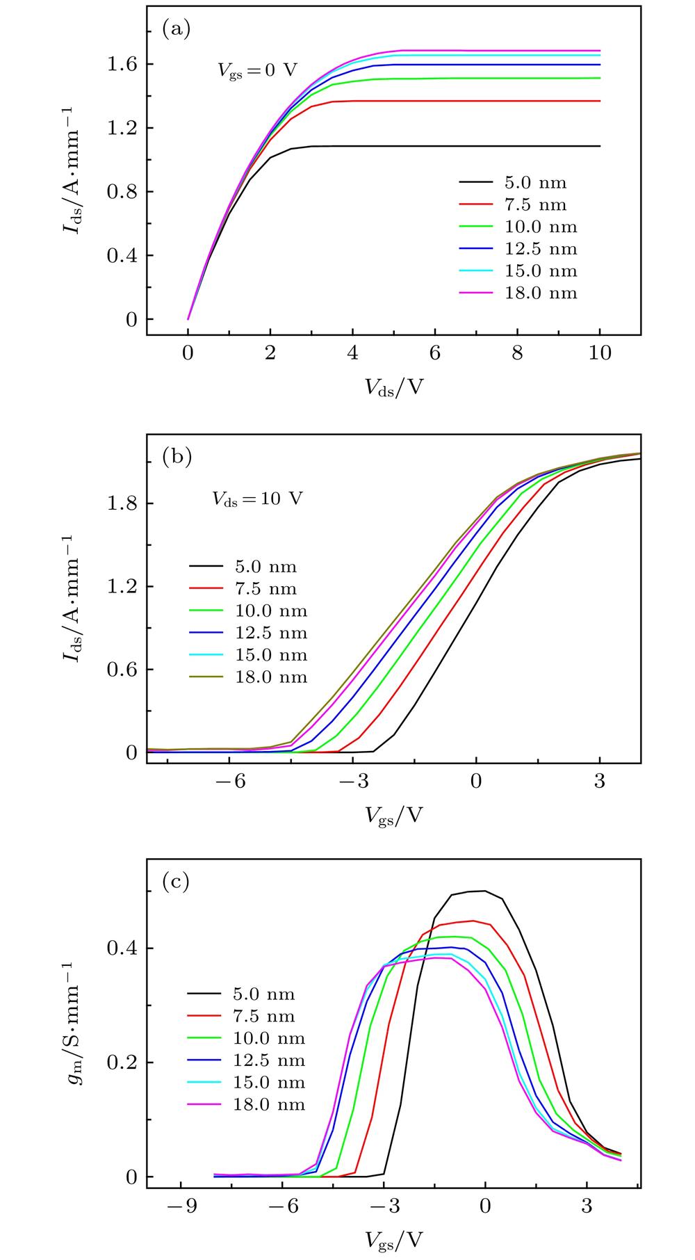
    Fig. 2. (a) Output characteristics, (b) transfer characteristics, and (c) transconductance curves of N-polar GaN/InAlN HEMTs with different GaN channel thicknesses.不同GaN沟道层厚度下, N极性面GaN/InAlN HEMT器件的(a) 输出特性、(b) 转移特性和(c) 跨导曲线
    (a) Conduction-band energy diagram and (b) electron distribution in N-polar GaN/InAlN HEMTs with different GaN channel thicknesses.不同GaN沟道层厚度下, N极性面GaN/InAlN HEMT器件栅极下方的(a)导带结构和(b)电子浓度分布图
    Fig. 3. (a) Conduction-band energy diagram and (b) electron distribution in N-polar GaN/InAlN HEMTs with different GaN channel thicknesses.不同GaN沟道层厚度下, N极性面GaN/InAlN HEMT器件栅极下方的(a)导带结构和(b)电子浓度分布图
    (a) Output characteristics, (b) transfer characteristics, and (c) transconductance curves of N-polar GaN/InAlN HEMTs with different InAlN back barrier thicknesses.不同InAlN背势垒层厚度下, N极性面GaN/InAlN HEMT器件的(a)输出特性、(b) 转移特性和(c)跨导曲线
    Fig. 4. (a) Output characteristics, (b) transfer characteristics, and (c) transconductance curves of N-polar GaN/InAlN HEMTs with different InAlN back barrier thicknesses.不同InAlN背势垒层厚度下, N极性面GaN/InAlN HEMT器件的(a)输出特性、(b) 转移特性和(c)跨导曲线
    (a) Conduction-band energy diagram and (b) electron distribution in N-polar GaN/InAlN HEMTs with different InAlN back barrier thicknesses. The inset in panel (a) is the partial enlarged conduction-band energy of the rectangular quantum well.不同InAlN背势垒层厚度下, N极性面GaN/InAlN HEMT器件栅极下方的(a)导带结构(内插图为三角势阱处导带结构的局部放大图), 以及(b) 电子浓度分布图
    Fig. 5. (a) Conduction-band energy diagram and (b) electron distribution in N-polar GaN/InAlN HEMTs with different InAlN back barrier thicknesses. The inset in panel (a) is the partial enlarged conduction-band energy of the rectangular quantum well.不同InAlN背势垒层厚度下, N极性面GaN/InAlN HEMT器件栅极下方的(a)导带结构(内插图为三角势阱处导带结构的局部放大图), 以及(b) 电子浓度分布图
    Yan-Li Liu, Wei Wang, Yan Dong, Dun-Jun Chen, Rong Zhang, You-Dou Zheng. Effect of structure parameters on performance of N-polar GaN/InAlN high electron mobility transistor[J]. Acta Physica Sinica, 2019, 68(24): 247203-1
    Download Citation