
Yaoran Huang, Taojie Zhou, Mingchu Tang, Guohong Xiang, Haochuan Li, Mickael Martin, Thierry Baron, Siming Chen, Huiyun Liu, Zhaoyu Zhang, "Highly integrated photonic crystal bandedge lasers monolithically grown on Si substrates," Chin. Opt. Lett. 20, 041401 (2022)
- Chinese Optics Letters
- Vol. 20, Issue 4, 041401 (2022)
Abstract
1. Introduction
Advanced microscale silicon photonics technology has emerged as a promising candidate for the next-generation chip-scale data communication network due to its unique advantages of low cost, high integration density, high speed, and energy efficiency[
Meanwhile, defect-free photonic crystal bandedge laser arrays enable a large-area coherent oscillation, so a large number of attractive applications have been derived[
In this paper, we demonstrate InAs/GaAs QD square lattice photonic crystal bandedge lasers monolithically grown on an on-axis Si (001) substrate with ultra-low lasing threshold under 632.8 nm He–Ne gas laser source at room temperature. This square lattice photonic crystal bandedge laser on Si can be a promising candidate for the coherent light source for Si photonics due to its low threshold characteristic and potential capability for high-power output.
Sign up for Chinese Optics Letters TOC. Get the latest issue of Chinese Optics Letters delivered right to you!Sign up now
2. Device Fabrication
The doping-free CMOS-compatible on-axis Si (001) substrates are offered for the monolithic growth of InAs/GaAs QD photonic crystal bandedge lasers[
![]()
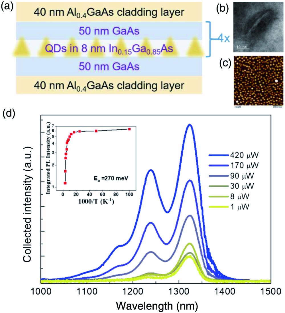
Figure 1.(a) Schematic epitaxial structure of the active region with total thickness of ∼ 362 nm. (b) A high-resolution TEM image of a single InAs QD. (c) An AFM image of uncapped InAs/GaAs QDs. (d) Collected PL spectra of the as-grown structure under various input optical powers at room temperature. Inset: temperature dependent integrated PL intensity.
Figure 2(a) shows the schematic figure of the photonic crystal bandedge lasers monolithically grown on an on-axis Si (001) substrate, and the lattice constant
![]()
Figure 2.(a) Schematic diagram of the fabricated InAs/GaAs QD bandedge laser directly grown on an on-axis Si (001) substrate. The lattice constant and radius of air holes are a and r, respectively. (b) An SEM image of fabricated photonic crystal bandedge cavity.
The fabrication processes of this bandedge laser are presented with these steps. First, plasma-enhanced chemical vapor deposition (PECVD) was used for depositing
3. Discussion
The dispersion relation diagram and the corresponding eigen-field profiles were calculated by MIT photonic bands (MPBs) based on the plane-wave expansion method[
![]()
Figure 3.(a) Dispersion relation diagram of TE-like states for the photonic crystal bandedge cavity with the parameters of r/a = 0.35 and the slab thickness of 1.05a. The inset shows the irreducible Brillouin zone. The shaded blue region indicates the light cone, and the purple area represents the gain region of as-grown QDs. High symmetry points with low group velocity within the gain region are marked as X2, M1, and M2. (b) The corresponding calculated hertz (Hz) field profiles.
A µ-PL system setup was used to characterize the fabricated photonic crystal bandedge lasers. We optically pumped the bandedge cavity at room temperature with a standard 632.8 nm He–Ne gas laser as the pumping source, whose standard Gaussian spot size is around 3 µm. The PL spectrum of this cavity with
![]()
Figure 4.(a) Emission spectrum of the fabricated photonic crystal bandedge laser, the pump power is 49.2 µW. Lasing modes of M1, X2, and M2 can be determined by the spectral positions. (b)–(d) The L-L curve and FWHM as a function of input power for three lasing modes M1, X2, and M2, respectively.
4. Conclusion
In conclusion, we have demonstrated InAs/GaAs QD square lattice photonic crystal bandedge lasers monolithically grown on on-axis Si (001) substrates. The lasers operated under continuous-wave optical pumping at room temperature. An ultra-low lasing threshold was observed in a multi-mode lasing operation. With further structure design or optimized plasma-etching profiles, a single mode lasing emission is feasible. The demonstrated photonic crystal bandedge lasers monolithically grown on the Si substrate are a promising candidate as a large-scale coherent light source for Si photonics.
References
[1] D. Thomson, A. Zilkie, J. E. Bowers, T. Komljenovic, G. T. Reed, L. Vivien, D. Marris-Morini, E. Cassan, L. Virot, J.-M. Fédéli, J.-M. Hartmann, J. H. Schmid, D.-X. Xu, F. Boeuf, P. O’Brien, G. Z. Mashanovich, M. Nedeljkovic. Roadmap on silicon photonics. J. Opt., 18, 073003(2016).
[2] M. Asghari, A. V. Krishnamoorthy. Energy-efficient communication. Nat. Photonics, 5, 268(2011).
[3] S. Chen, W. Li, J. Wu, Q. Jiang, M. Tang, S. Shutts, S. N. Elliott, A. Sobiesierski, A. J. Seeds, I. Ross, P. M. Smowton, H. Liu. Electrically pumped continuous-wave III-V quantum dot lasers on silicon. Nat. Photonics, 10, 307(2016).
[4] R. Alcotte, M. Martin, J. Moeyaert, R. Cipro, S. David, F. Bassani, F. Ducroquet, Y. Bogumilowicz, E. Sanchez, Z. Ye, X. Y. Bao, J. B. Pin, T. Baron. Epitaxial growth of antiphase boundary free GaAs layer on 300 mm Si (001) substrate by metalorganic chemical vapour deposition with high mobility. APL Mater., 4, 046101(2016).
[5] M. Tang, S. Chen, J. Wu, Q. Jiang, K. Kennedy, P. Jurczak, M. Liao, R. Beanland, A. Seeds, H. Liu. Optimizations of defect filter layers for 1.3-µm InAs/GaAs quantum-dot lasers monolithically grown on Si substrates. IEEE J. Sel. Top. Quantum Electron., 22, 50(2016).
[6] H. Liu, T. Wang, Q. Jiang, R. Hogg, F. Tutu, F. Pozzi, A. Seeds. Long-wavelength InAs/GaAs quantum-dot laser diode monolithically grown on Ge substrate. Nat. Photonics, 5, 416(2011).
[7] A. Lee, Q. Jiang, M. Tang, A. Seeds, H. Liu. Continuous-wave InAs/GaAs quantum-dot laser diodes monolithically grown on Si substrate with low threshold current densities. Opt. Express, 20, 22181(2012).
[8] D. Jung, J. Norman, M. Kennedy, C. Shang, B. Shin, Y. Wan, A. C. Gossard, J. E. Bowers. High efficiency low threshold current 1.3 µm InAs quantum dot lasers on on-axis (001) GaP/Si. Appl. Phys. Lett., 111, 122107(2017).
[9] Y. Wan, Q. Li, A. Y. Liu, A. C. Gossard, J. E. Bowers, E. L. Hu, K. M. Lau. Optically pumped 1.3 µm room-temperature InAs quantum-dot micro-disk lasers directly grown on (001) silicon. Opt. Lett., 41, 1664(2016).
[10] T. Zhou, M. Tang, G. Xiang, B. Xiang, S. Hark, M. Martin, M.-L. Touraton, T. Baron, Y. Lu, S. Chen, H. Liu, Z. Zhang. Ultra-low threshold InAs/GaAs quantum dot microdisk lasers on planar on-axis Si (001) substrates. Optica, 11, 430(2020).
[11] T. Zhou, M. Tang, G. Xiang, X. Fang, X. Liu, B. Xiang, S. Hark, M. Martin, T. Baron, S. Pan, J.-S. Park, Z. Liu, S. Chen, Z. Zhang, H. Liu. Continuous-wave quantum dot photonic crystal lasers grown on on-axis Si (001). Nat. Commun., 11, 977(2020).
[12] T. Zhou, M. Tang, H. Li, Z. Zhang, Y. Cui, J.-S. Park, M. Martin, T. Baron, S. Chen, H. Liu, Z. Zhang. Single-mode photonic crystal nanobeam lasers monolithically grown on Si for dense integration. IEEE J. Sel. Top. Quantum Electron., 28, 1501906(2021).
[13] H.-Y. Ryu, S.-H. Kwon, Y.-J. Lee, Y.-H. Lee, J.-S. Kim. Very-low-threshold photonic band-edge lasers from free-standing triangular photonic crystal slabs. Appl. Phys. Lett., 80, 3476(2002).
[14] S.-H. Kwon, H.-Y. Ryu, G.-H. Kim, Y.-H. Lee, S.-B. Kim. Photonic bandedge lasers in two-dimensional square-lattice photonic crystal slabs. Appl. Phys. Lett., 83, 3870(2003).
[15] H.-Y. Lu, S.-C. Tian, C.-Z. Tong, L.-J. Wang, J.-M. Rong, C.-Y. Liu, H. Wang, S.-L. Shu, L.-J. Wang. Extracting more light for vertical emission: high power continuous wave operation of 1.3-µm quantum-dot photonic-crystal surface-emitting laser based on a flat band. Light Sci. Appl., 8, 108(2019).
[16] S. Noda, K. Kitamura, T. Okino, D. Yasuda, Y. Tanaka. Photonic-crystal surface-emitting lasers: review and introduction of modulated-photonic crystals. IEEE J. Sel. Top. Quantum Electron., 23, 4900107(2017).
[17] H. Y. Liu, I. R. Sellers, T. J. Badcock, D. J. Mowbray, M. S. Skolnick, K. M. Groom, M. Gutierrez, M. Hopkinson, J. S. Ng, J. P. R. David, R. Beanland. Improved performance of 1.3 µm multilayer InAs quantum-dot lasers using a high-growth-temperature GaAs spacer layer. Appl. Phys. Lett., 85, 704(2004).
[18] S. G. Johnson, J. D. Joannopoulos. Block-iterative frequency-domain methods for Maxwell’s equations in a planewave basis. Opt. Express, 8, 173(2001).


Set citation alerts for the article
Please enter your email address

© Copyright 2018-2021 | Chinese Laser Press. All Rights Reserved 沪ICP备15018463号-20