Xue Yang, Huilai Sun, Duanmu Yue, Jianlin Sun. Research Progress of Femtosecond Laser Fabrication of Microlens Array[J]. Laser & Optoelectronics Progress, 2021, 58(5): 0500005
Search by keywords or author
- Laser & Optoelectronics Progress
- Vol. 58, Issue 5, 0500005 (2021)
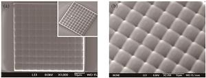
![SEM image and its partial enlarged view of 100% fill factor square microlens array[32]. (a)SEM image; (b) partially enlarged view](/richHtml/lop/2021/58/5/0500005/img_1.jpg)
Fig. 1. SEM image and its partial enlarged view of 100% fill factor square microlens array[32]. (a)SEM image; (b) partially enlarged view
![Femtosecond laser two-photon polymerization technology to prepare optical flow microlens array[33]. (a) Wet etching-assisted femtosecond laser fabrication of 3D embedded glass microchannels; (b) two-photon polymerization technology for integration of a polymer center-pass microlens array; (c) cell counting by observing the intensity variations at the focal spots of a microlens array, when a cell passes across a microlens, the intensity dips; (d) top view and (e) magnified SEM images of a center-pass combined microlens array fabricated by two-photon polymerization technology; (f) M-shaped limiting wall with 9 μm aperture to control the passage of cells above the center of the microlens](/richHtml/lop/2021/58/5/0500005/img_2.jpg)
Fig. 2. Femtosecond laser two-photon polymerization technology to prepare optical flow microlens array[33]. (a) Wet etching-assisted femtosecond laser fabrication of 3D embedded glass microchannels; (b) two-photon polymerization technology for integration of a polymer center-pass microlens array; (c) cell counting by observing the intensity variations at the focal spots of a microlens array, when a cell passes across a microlens, the intensity dips; (d) top view and (e) magnified SEM images of a center-pass combined microlens array fabricated by two-photon polymerization technology; (f) M-shaped limiting wall with 9 μm aperture to control the passage of cells above the center of the microlens
Fig. 3. SLM-based femtosecond laser two-photon polymerization processing system[37]
Fig. 4. Wet etching assisted femtosecond laser preparation of microlens array[46]. (a) Schematic of processing; (b) SEM images of closely packed rectangular microlens arrays, and the inset is partially enlarged view;(c) hexagonal microlens arrays, and the inset is partially enlarged view
Fig. 5. Wet etching assisted femtosecond laser processing combined with hot embossing process to prepare artificial compound eye[47]
Fig. 6. Spatial light modulator assisted femtosecond laser preparation of 3D close-packed compound microlens array[48]. (a) Schematic of holographic femtosecond laser processing system based on SLM; (b) top view of the close-packed compound microlens with 3D arrangement; (c)(d) 3D topography and side view of the micro-concave lens in the close-packed compound microlens; (e) schematic of microlens array imaging system; (f)(g) microlens array imaging performance, eccentricity (f) and center (g) show clear images, respectively
Fig. 7. Wet etching assisted femtosecond laser processing combined with femtosecond laser direct writing to prepare PDMS microlens arrays[49]. (a)‒(c) Manufacturing process of microlens array; (d) SEM image of microlens array; (e) 3D contour of textured microlens array; (f) optical image of textured microlens array; (g) optical image of smooth microlens array
Fig. 8. Dry etching assisted femtosecond laser manufacturing silicon concave structure[50]. (a) Schematic of dry etching assisted femtosecond laser manufacturing silicon concave structure, and the inset is SEM image of the silicon concave structure; (b) schematic of cross-sectional profiles of the concave structures to illustrate the etching process
Fig. 9. Fabrication and characterization of a microlens[51]. (a) Manufacture of sapphire concave microlenses by dry etching assisted femtosecond laser, (i) laser irradiation for the fabrication of microholes, (ii) rapid removal of laser-modified regions in the initial etching stage, (iii) formation of concave microlens after increasing the etching time; (b) relationship between the diameter and height of sapphire concave microlens and etching time; (c)‒(e) SEM images of a microhole, and etching for 0 min, 30 min, and 180 min, respectively; (f) cross-section profiles of microstructures in Fig.9 (c)‒(e) and the fitting curve of the microlens in Fig. 9 (e)
Fig. 10. Schematic of TOMBO compound eye imaging system[52]. (a) TOMBO system; (b) optical system of TOMBO architecture
Fig. 11. Schematic of Shack-Hartmann sensor[53]
Fig. 12. Schematic of light field camera[54]
Fig. 13. Schematic of beam homogenization system of microlens array based on excimer laser[55]
Fig. 14. Schematic of solid-phase PCR on a supercritical angle fluorescent microlens array[56]
Fig. 15. Schematic of collimated OLED light source[57]. (a) Structure; (b) geometric parameters
Fig. 16. Schematic of cell detection based on integrated optical flow microchip[58]
Fig. 17. Miniature concave lens with aspheric profile[59].(a) (b) SEM images of miniature concave lenses with an average diameter of 20 μm and 30 μm; (c) (d) 3D intensity distribution and cross-sectional profile of microlens array
Fig. 18. Wide FOV of artificial compound eyes[47]. (a)‒(c) Output imaging of artificial compound eyes at 0°, 30°, and 60° angle of incidence; (d) intensity distribution along x and y axes for θ equal to 0°, and the inset is a microscope image of a single focal spot; (e) (f) comparison of x- and y-direction intensity distributions under incident angles of 0°, 30°, and 60°
Fig. 19. Superhydrophobic microfluidic array[60].(a)PDMS surface composed of both the superhydrophobic microfluidic arrays domain and normal microfluidic arrays domain; (b) spraying a jet of water onto the whole sample surface randomly; (c) photography of contaminated samples; (d) photography of the polluted surface after water droplet rolling away

Set citation alerts for the article
Please enter your email address


