
Lipeng Xia, Yuheng Liu, Peiji Zhou, Yi Zou. Advances in mid-infrared integrated photonic sensing system (Invited)[J]. Infrared and Laser Engineering, 2022, 51(3): 20220104
- Infrared and Laser Engineering
- Vol. 51, Issue 3, 20220104 (2022)
![Mid-infrared absorption spectra for common gases[5]](/richHtml/irla/2022/51/3/20220104/img_1.jpg)
Fig. 1. Mid-infrared absorption spectra for common gases[5]
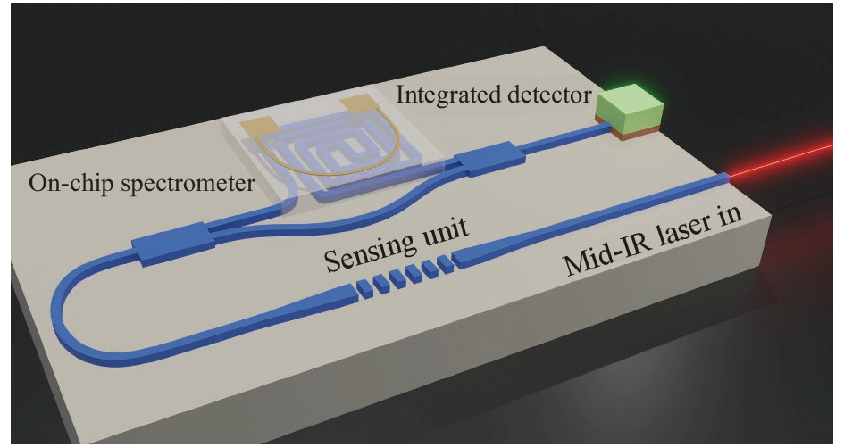
Fig. 2. Mid-infrared integrated on-chip sensing system
Fig. 3. Mid-IR waveguide sensing units. (a) The germanium strip waveguide designed by Yu-Chi Chang et al. for cocaine sensing[42]; (b) SEM image of the air-clad pedestal silicon waveguide designed by Pao Tai Lin et al.[43]; (c) Microscope image of the monolithic integrated sensor designed by Yi Zou et al. using germanium waveguides[44]; (d) The strip waveguide designed by Neetesh Singh et al. for D2O sensing[6]; (e) The suspended silicon waveguide designed by Floria Ottonello-Briano et al. for CO2 sensing (top) and the support structure of the designed suspended silicon waveguide (bottom)[8]
Fig. 4. Mid-IR slot waveguide & iHWG sensing units. (a) SEM image of the mid-infrared slot waveguide designed by Nedeljkovic et al. [46]; (b) Simulation result of the mid-infrared slot waveguide by the same team in 2015[47]; (c) The “silicon-liquid-silicon” nanofluidic slot-waveguide based on-chip chemical sensor designed by Pao Tai Lin et al[48]; (d) Schematic of a spiral iHWG etched on silicon substrate designed by Shaonan Zheng et al (top), the cross section of the spiral iHWG (bottom left) and the schematic assembly of LED, iHWG, and PD (bottom right)[50]
Fig. 5. Mid-IR ring resonator based sensing units. (a) SEM image of the racetrack resonator designed by Benedetto Troia et al[58]; (b) Cascaded ring resonators for acetone/IPA sensing designed by Yuhua Chang et al[59]; (c) The ring resonator based N2O sensor designed by Clinton J Smith et al[62] ; (d) The sensor on a CaF2 substrate based on ring resonators designed by Yu Chen et al[63]
Fig. 6. Mid-IR photonic crystal waveguide sensing units. (a) The schematic of the mid-infrared silicon-on-sapphire photonic crystal waveguide coupled microcavity designed by Yi Zou et al[72]; (b) The mid-infrared photonic crystal waveguide based TEP sensor designed by the same group: SEM image of the holey photonic crystal waveguide (left) and SEM image of the slotted photonic crystal waveguide (right) [73] ; (c) The schematic of the ethanol sensor based on photonic crystal designed by Ali Rostamian et al[74]
Fig. 7. Mid-IR in-plane sensing units based on materials except group-IV. (a) The Ta2O5 waveguide designed by Marek Vlk et al for acetylene sensing[85]; (b) SEM image of chalcogenide waveguide designed by Mingquan Pi et al for CO2 sensing (left) and the sensor schematic (right)[90]; (c) Schematic of the bendable AlN-on-borosilicate waveguide based chemical sensor (left) and cross-section (right) designed by Tiening Jin et al[92]
Fig. 8. Scheme of the monolithically integrated plasmonic waveguide sensor designed by Benedikt Schwarz et al[34]
Fig. 9. Mid-IR out-of-plane sensors. (a) The flexible surface plasmon resonance biochemical sensor based on PDMS materials designed by Chiao-Yun Chang et al[93]; (b) The dual-resonance Mid-IR MPA multifunctional chemical sensing platform designed by Dongxiao Li et al[17]; (c) The multi-resonance metasurface based label-free biosensor designed by Daniel Rodrigo et al[108]; (d) Schematic of the biosensor for passively capturing analyte molecules designed by Xianglong Miao et al[117]; (e) Schematic of the cross-section of the graphene-metallic metasurface biosensor designed by Yibo Zhu et al[119]
Fig. 10. Reconstructive spectrometers. (a) Reconstructive spectrometer simulation based on inverse design proposed by Tianran Liu et al[135]; (b) Schematic of a tunable reconstructive spectrometer based on black phosphorus proposed by Shaofan Yuan et al[136]; (c) Reconstructive spectrometer with a multi-lattice periodic array of metal nano-aluminum disks designed by Hwa-Seub Lee et al[137]
Fig. 11. Spatial heterodyne Fourier transform spectrometers. (a) SEM image of a MZI array spectrometer designed by Milos Nedeljkovic et al[140]; (b) SEM image of a MZI array spectrometer designed by Qiankun Liu et al [142] ; (c) Schematic diagram of thermo-optical scanning MZI array spectrometer designed by Miguel Montesinos-Ballester et al[143]; (d) Schematic diagram and SEM image of a micromechanical structure-type Fourier transform spectrometer designed by Alaa Fathy et al[144]
Fig. 12. Principle and structure diagram of the dual-comb spectrometer. (a) Frequency domain and time domain schematic of the dual-comb spectrometer[147]; (b) Schematic of the on-chip dual-comb spectrometer based on the optical parametric oscillator by Mengjie Yu et al[150];(c) Schematic and optical microscope image of a nonlinear dissipative Kerr soliton dual-comb spectrometer in the near-infrared by Tong Lin et al[151]
Fig. 13. Optical response range of some absorbing materials
Fig. 14. Mid-IR integrated photodetectors. (a) Schematic of the integrated InSb photodetector on Si substrate reported by Bowen Jia et al[160]; (b) Schematic of the high-performance InAs/InAsSb superlattice mid-infrared detector directly grown on Si substrate proposed by Evangelia Delli et al[161]; (c) Schematic of the GeSn mid-infrared detector proposed by Cong Hui et al[163]; (d) Schematic of the GeSn mid-infrared detector proposed by Huong Tran et al[164] ; (e) Schematic of a graphene-based heterostructure photodetector proposed by Xiaomu Wang et al[165]; (f) Schematic of the photodetector based on chalcogenide glass-on-graphene waveguide integration proposed by HongTao Lin et al[24]; (g) Schematic of the metal-graphene-metal waveguide integrated detector reported by Zhibo Qu et al[166]; (h) Schematic of the waveguide-integrated black phosphorus mid-infrared detector proposed by Li Huang et al[167]
|
Table 1. Characteristics of the Mid-IR in-plane sensing units
|
Table 2. Characteristics of the mid-IR out-of-plane SPR sensors
|
Table 3. Summary of reconstructive spectrometers
|
Table 4. Summary of spatial heterodyne Fourier transform spectrometers
|
Table 5. Summary of dual-comb spectrometers
| ||||||||||||||||||||||||||||||||||||||||||||||||||||||||||||||||||||||
Table 6. Summary of mid-IR integrated photodetectors

Set citation alerts for the article
Please enter your email address
© Copyright 2018-2021 | Chinese Laser Press. All Rights Reserved 沪ICP备15018463号-20