
Wenhao Geng, Guang Yang, Xuqing Zhang, Xi Zhang, Yazhe Wang, Lihui Song, Penglei Chen, Yiqiang Zhang, Xiaodong Pi, Deren Yang, Rong Wang. Identification of subsurface damage of 4H-SiC wafers by combining photo-chemical etching and molten-alkali etching[J]. Journal of Semiconductors, 2022, 43(10): 102801
- Journal of Semiconductors
- Vol. 43, Issue 10, 102801 (2022)
![(Color online) (a) AFM image of the CMP-treated 4H-SiC wafer, (b) distribution and (c) density of defects of the CMP-treated 4H-SiC wafer, and (d) DIC and UV-PL images of the same PL-Black defect site [the black box in (b)] of the Si-face of the CMP-treated 4H-SiC wafer.](/richHtml/jos/2022/43/10/102801/102801-1.jpg)
Fig. 1. (Color online) (a) AFM image of the CMP-treated 4H-SiC wafer, (b) distribution and (c) density of defects of the CMP-treated 4H-SiC wafer, and (d) DIC and UV-PL images of the same PL-Black defect site [the black box in (b)] of the Si-face of the CMP-treated 4H-SiC wafer.
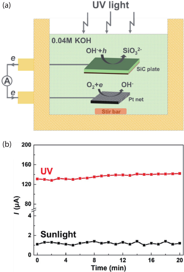
Fig. 2. (Color online) (a) Schematic diagram showing the setup of the photo-chemical etching of 4H-SiC. (b) The current of 4H-SiC during the photo-chemical etching under the UV and sunlight illumination.
Fig. 3. (a) Differential interference contrast (DIC) optical microscopy image, (b) SEM image, (c) AFM image, and (d) height of the ridge-like defect in the photo-chemically etched Si-face of 4H-SiC.
Fig. 4. (Color online) (a) Optical microscopy image, (b) Raman spectra, and Raman mappings based on the intensity of peaks located at (c) 204, (d) 776, and (e) 984 cm–1 across the ridge-like defect in the photo-chemically etched Si-face of 4H-SiC.
Fig. 5. (Color online) (a) Schematic diagram of molten-KOH etching of the photo-chemically etched Si-face of 4H-SiC. (b, c) DIC images obtained with the molten-KOH etching with 3 and 30 min, respectively. The insets show the local SEM images in the red dotted boxes.
Fig. 6. (Color online) Cross-section schematic diagrams showing the Si-face of 4H-SiC after the (a) fine-lapping, (b) CMP, (c) photo-chemical etching and (d) molten-KOH etching.

Set citation alerts for the article
Please enter your email address
© Copyright 2018-2021 | Chinese Laser Press. All Rights Reserved 沪ICP备15018463号-20