Abstract
In this work, we propose to reveal the subsurface damage (SSD) of 4H-SiC wafers by photo-chemical etching and identify the nature of SSD by molten-alkali etching. Under UV illumination, SSD acts as a photoluminescence-black defect. The selective photo-chemical etching reveals SSD as the ridge-like defect. It is found that the ridge-like SSD is still crystalline 4H-SiC with lattice distortion. The molten-KOH etching of the 4H-SiC wafer with ridge-like SSD transforms the ridge-like SSD into groove lines, which are typical features of scratches. This means that the underlying scratches under mechanical stress give rise to the formation of SSD in 4H-SiC wafers. SSD is incorporated into 4H-SiC wafers during the lapping, rather than the chemical mechanical polishing (CMP).In this work, we propose to reveal the subsurface damage (SSD) of 4H-SiC wafers by photo-chemical etching and identify the nature of SSD by molten-alkali etching. Under UV illumination, SSD acts as a photoluminescence-black defect. The selective photo-chemical etching reveals SSD as the ridge-like defect. It is found that the ridge-like SSD is still crystalline 4H-SiC with lattice distortion. The molten-KOH etching of the 4H-SiC wafer with ridge-like SSD transforms the ridge-like SSD into groove lines, which are typical features of scratches. This means that the underlying scratches under mechanical stress give rise to the formation of SSD in 4H-SiC wafers. SSD is incorporated into 4H-SiC wafers during the lapping, rather than the chemical mechanical polishing (CMP).Introduction
4H silicon carbide (4H-SiC) wafers have recently shown great potential for the development of high-power electronics, high-frequency electronics and quantum information technologies owing to the high saturated electron velocity, high breakdown field and high thermal conductivity of 4H-SiC[1,2]. 4H-SiC wafers are produced from 4H-SiC single-crystal boules using the ordinal slicing, lapping and chemical mechanical polishing (CMP) processes. Due to the high hardness and brittleness of 4H-SiC, the processing of 4H-SiC wafers introduces high density of damages, such as cracks, dislocations, phase transitions, and so on.[3,4]. As the last processing step, CMP should ideally remove all the damages and create smooth surface with extremely small roughness[5]. However, it has been found that optically invisible damages often exist in the subsurface of a 4H-SiC wafer after CMP, and this damage can be shown up as scratch-like structures via H2 etching[6,7], laser duration[8], and inductivity coupled plasma treatment[9]. Subsurface damage (SSD) serves as the nucleation site of threading dislocations during the homoepitaxy of 4H-SiC, which are detrimental to the performance of 4H-SiC devices[10,11]. It is still under debate whether SSD is created by insufficient removal of lapping-induced damages during CMP, or by imperfect CMP that creates SSD in 4H-SiC wafers[12,13]. This issue clearly limits the optimization of the processing of 4H-SiC wafers. Therefore, it is critical to identify the nature of SSD and prevent its formation during the processing to improve the quality of 4H-SiC wafers.
Both non-destructive and destructive approaches have been developed to study the nature of SSD in semiconductor wafers. Non-destructive approaches including X-ray diffraction, laser scattering and acoustic probing are promising options for the detection of the SSD, but they are incapable of detecting the thickness of the SSD, and its distance away from the surface[14,15]. The destructive approaches, such as taper-polishing, cross-sectional microscopy and chemical etching, are able to directly and accurately detect the SSD[16-21]. However, taper-polishing and cross-sectional microscopy are time-consuming and highly complex[22]. Chemical etching only determines the distance of a SSD from the surface of semiconductors[17]. It is known that photo-chemical etching is capable of revealing linear defects and planar defects in wide-bandgap semiconductors[23-26]. During photo-chemical etching, UV-excited holes participate in the oxidation and removal of the perfect region of a wafer. UV-excited electrons and holes recombine at the linear defects and planar defects[27-29]. Therefore, photo-chemical etching is capable of revealing dislocations and planar defects by removing the perfect region of semiconductor wafers.
In this work, we propose to reveal the SSD in 4H-SiC by the photo-chemical etching, and identify the nature of SSD by molten-alkali etching. Under UV illumination, the SSD acts as a photoluminescence (PL)-black defect. The selective photo-chemical etching is carried out in dilute KOH solution via short-circuiting 4H-SiC to a platinum net. By removing perfect 4H-SiC above and around the SSD, the SSD is then revealed as a ridge-like defect. Micro-Raman measurements indicate that the crystalline character of the ridge-like SSD is still 4H-SiC, with only lattice distortions. Molten-KOH etching of the 4H-SiC wafer with ridge-like SSD transforms the ridge-like SSD into a groove line, which is typical features of a underlying scratch. Since the width of the ridge-like SSD is similar to the average diameters of the diamond abrasive particles during the lapping, we propose that the SSD of 4H-SiC wafers is induced during the lapping by the scratching of diamond abrasive particles. Our work indicates that the SSD is incorporated in 4H-SiC wafers during the lapping, rather than the CMP. To eliminate SSD in 4H-SiC wafers, efforts should be devoted to optimizing the lapping process or increase the duration of the CMP process.
Experimental section
Materials and methods
Nitrogen (N)-doped 4H-SiC boules were grown by the physical vapor transport (PVT) technology, with temperature ranging from 2200 to 2300 °C, and pressure ranging from 1 to 10 mbar. High purity N2 was mixed in the argon (Ar) gas as the doping source. During the processing of 4H-SiC wafers, the 4.0° off-axis sliced wafers are coarse-lapped, fine-lapped and chemical-mechanical polished successively, in which the average diameters of diamond abrasives during the coarse-lapping and fine-lapping are 3.0 and 1.0μm, respectively. The chemical mechanical polishing process is then followed by using the alumina abrasives (200–300 nm) and silica abrasives (50–70 nm).
The CMP-treated 4H-SiC wafers were cut into 0.5 × 1.0 cm2 samples and sequentially washed by ultrasonic acetone, ethanol and deionized water for 15 min. The 4H-SiC samples were finally immersed in HF solution to remove surface oxides. Before the photo-chemical etching, a 100 nm-thick titanium (Ti) was evaporated on the C face of the 4H-SiC sample to enhance the separation of UV-excited electrons and holes. A 500 W Hg lamp was used as the UV-light source, which vertically illuminates the Si surface of 4H-SiC. The 4H-SiC electrode was directly connected to a platinum (Pt)-counter electrode. The photo-chemical etching experiment was carried out in 0.04 M KOH solution. The molten-alkali etching of the 4H-SiC samples were carried out at 550 °C in a Ni crucible, with the 4H-SiC samples placed in a Ni-wire meshes. The etching durations for N-doped 4H-SiC sample was 3 and 30 min, respectively.
Characterization
Morphological distribution for defects of the CMP-treated 4H-SiC wafers was measured and counted by the Lasertec SICA88 using a Nomarski confocal differential interference contrast microscope for surface imaging and UV photoluminescence (UV-PL) mapping. The excitation wavelength for the UV-PL measurements was 313 nm. The surface morphologies after etching were examined using differential interference contrast (DIC) optical microscopy, scanning electron microscopy (SEM) and atomic force microscope (AFM). Micro-Raman spectroscopy was carried out using a WITec Alpha300R micro-Raman spectrometer with a 75 mW green-diode laser operating at 532 nm with the exposure time of 20 s and spot diameter of 1.5μm.
Results and discussion
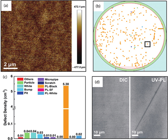
As shown inFig. 1(a), the CMP processing yields a flat and smooth 4H-SiC wafer. The surface roughness for the Si-face of the 4H-SiC wafer is 0.11 nm, which meets the requirement of subsequent homoepitaxy. The distribution and density of defects at the Si-face of the CMP-treated 4H-SiC wafer are presented inFigs. 1(b) and1(c), respectively. Although scratches, pits, bumps, particles and other defects are almost cleaned up after CMP, the UV-PL image shows that high density (5.38 cm–2) of PL-Black defects appear at the Si-face of the CMP-treated 4H-SiC wafer. As shown inFig. 1(d), the PL-Black defects are invisible under optical microscopy but appear as straight lines in the UV-PL measurements. This indicates that the SSD appears at the CMP-treated 4H-SiC wafer.
![(Color online) (a) AFM image of the CMP-treated 4H-SiC wafer, (b) distribution and (c) density of defects of the CMP-treated 4H-SiC wafer, and (d) DIC and UV-PL images of the same PL-Black defect site [the black box in (b)] of the Si-face of the CMP-treated 4H-SiC wafer.](/Images/icon/loading.gif)
Figure 1.(Color online) (a) AFM image of the CMP-treated 4H-SiC wafer, (b) distribution and (c) density of defects of the CMP-treated 4H-SiC wafer, and (d) DIC and UV-PL images of the same PL-Black defect site [the black box in (b)] of the Si-face of the CMP-treated 4H-SiC wafer.
To clarify the nature of the PL-Black SSD, the photo-chemical etching of the CMP-treated 4H-SiC was carried out in 0.04 M KOH solution.Fig. 2(a) schematically shows the setup for the photo-chemical etching. The 4H-SiC sample is connected to the Pt sheet by short circuiting. The onset potential of the oxygen reduction reaction at Pt is more positive than that of the photoanodic oxidation of 4H-SiC, which initiates the photo-etching reaction[30]. During photo-chemical etching of the perfect region of 4H-SiC, the UV-generated electron-hole pairs are separated by the electric field of the surficial space-charge layer. The UV-generated electrons (e) transporting to the Pt net via the circuit are captured by the dissolved oxygen, and form OH– species by the reaction: O2 + 2H2O + 4e → 4OH–. The holes (h) are left at the Si-face of the 4H-SiC sample and participates in the oxidation and dissolution of the perfect region of 4H-SiC by the reaction: SiC + 10OH– + 8h →
+ CO2↑ + 5H2O[29]. As shown inFig. 2(b), the etching current for the Si-face of 4H-SiC remains at 130μA under UV illumination, which is much higher than the current of that under natural sunlight illumination (1μA), indicating the strong etching of 4H-SiC.
Figure 2.(Color online) (a) Schematic diagram showing the setup of the photo-chemical etching of 4H-SiC. (b) The current of 4H-SiC during the photo-chemical etching under the UV and sunlight illumination.
Because the UV-generated electrons and holes would recombine at the defects of 4H-SiC[27,28], the PL-Black SSD on the Si-face of CMP-treated 4H-SiC are preserved as straight ridges during the photo-chemical etching [Fig. 3(a) and3(b)], which are consistent with the UV-PL results [Fig. 1(d)]. After 20 min of photo-chemical etching, the width and height of the ridge-like defects are ~2μm and 82 nm, respectively [Figs. 3(c) and3(d)].
Figure 3.(a) Differential interference contrast (DIC) optical microscopy image, (b) SEM image, (c) AFM image, and (d) height of the ridge-like defect in the photo-chemically etched Si-face of 4H-SiC.
Micro-Raman spectroscopy is then used to investigate the crystalline properties and lattice distortions of the exposed ridge-like defects.Fig. 4(a) illustrates the distribution of two tested points on photo-chemical etched Si-face. As shown inFig. 4(b), the folded mode of the transverse acoustic branch (FTA) locating at 204 cm–1, as well as the folded modes of the transverse optical branches (FTO) locating at 776 and 796 cm–1, are observed in the ridge-like defect and the perfect 4H-SiC region. The folded mode of the longitudinal optical branches (FLO) shifts to 984 cm–1, as a result of N-doping[31]. This indicates that the polytype of the ridge-like defect is still 4H-SiC[32]. As shown inFigs. 4(c)–4(e), the micro-Raman mapping across the ridge-like defect indicates that the intensities of the FTA peak, FLO peak, and FTO peak of the ridge-like defect are all lower than that of the perfect region, which indicates the atomic displacement of the ridge-like SSD.
Figure 4.(Color online) (a) Optical microscopy image, (b) Raman spectra, and Raman mappings based on the intensity of peaks located at (c) 204, (d) 776, and (e) 984 cm–1 across the ridge-like defect in the photo-chemically etched Si-face of 4H-SiC.
To investigate the nature of the atomic displacement of the ridge-like SSD, molten-KOH etching is then carried out on the 4H-SiC that undergoes photo-chemical etching. After 3 min of molten-KOH etching at 550 °C, the ridge-like SSD changes into a groove line [Fig. 5(b), inset], which is due to the preferential etching along defects during the molten-KOH etching[33,34]. As the etching duration increases to 30 min [Fig. 5(c)], the groove line gradually becomes wider and shallower. According to results obtained by Zhanget al., the groove line is attributed to the underlying scratches[8,10]. In addition, some groove lines [in the red dotted box ofFigs. 5(b) and5(c)] gradually disappear due to the molten-KOH etching, which further demonstrates the characteristics of underlying scratches. This indicates that the underlying scratches induced by mechanical stresses give rise to the formation of SSD in 4H-SiC.
Figure 5.(Color online) (a) Schematic diagram of molten-KOH etching of the photo-chemically etched Si-face of 4H-SiC. (b, c) DIC images obtained with the molten-KOH etching with 3 and 30 min, respectively. The insets show the local SEM images in the red dotted boxes.
Finally, the origin of SSD on 4H-SiC wafers is discussed. During the processing of N-doped 4H-SiC wafers, 4.0° off-axis slicing, coarse lapping, fine lapping and CMP are successively carried out. The average diameters of diamond abrasives during the rough lapping and fine lapping are 3.0 and 1.0μm, respectively. According to the relationship between the damage depth (δ) and the size (d) of abrasives, 0.3d0.68 <δ < 2d0.85[16], the maximum damage depth on Si-face of 4H-SiC wafers induced by coarse lapping and fine lapping are calculated to be 5.1 and 2.0μm, respectively. To eliminate the damage caused by rough lapping and fine lapping, the material removal thicknesses of the Si-face of 4H-SiC during the fine lapping and CMP are 6.0 and 3.5μm, respectively. Zhuet al. performed molecule dynamics (MD) simulations to understand the deformation of 4H-SiC[35]. Except for cracks, distortion structures and amorphous structures have also been identified as the mechanical-processing induced defects [Fig. 6(a)]. The CMP process is carried out to remove the fine-lapping-induced surface damages and create an atomically smooth surface that is ready for the epitaxy of 4H-SiC thin films, while the underlying scratches still exist below the smooth Si-face and form the SSD [Fig. 6(b)]. The photo-chemical etching [Fig. 6(c)] and molten-alkali etching [Fig. 6(d)] are successively carried out to reveal and identify the nature of the SSD. The average width of the SSD is about 2μm, which is in the range of the diameter of the diamond abrasives during the fine lapping. Therefore, we conclude that SSD is induced by the scratch of diamond abrasive particles during the lapping. Furthermore, the abrasives of Al2O3 and SiO2 during the CMP is softer than 4H-SiC, which confirms that the SSD is not likely to be induced during CMP. This indicates that efforts should be devoted to optimize the lapping process to avoid the formation of scratches during the lapping, or to prolong the duration of the CMP process to sufficiently remove of the lapping-induced SSD.
Figure 6.(Color online) Cross-section schematic diagrams showing the Si-face of 4H-SiC after the (a) fine-lapping, (b) CMP, (c) photo-chemical etching and (d) molten-KOH etching.
Conclusion
In conclusion, we have systematically explored the nature and origin of SSD on the Si-face of CMP-treated 4H-SiC. By ultra-violet photoluminescence mapping on the Si-face, the SSD on the Si-face of CMP-treated 4H-SiC wafers are revealed as linear PL-Black defects. The layer-by-layer photo-chemical etching indicates that SSD appears in the form of ridges with a width of ~2μm. Further molten-KOH etching indicates that the SSD consists of a string of underlying scratches. We conclude that SSD is created during the lapping process, and further efforts should be devoted to optimize the lapping process to avoid the formation of scratches during the lapping or to prolong the duration of the CMP process to sufficiently remove lapping-induced SSD.
Acknowledgements
This work is supported by “Pioneer” and “Leading Goose” R&D Program of Zhejiang (Grant No. 2022C01021), National Key Research and Development Program of China (Grant No. 2018YFB2200101), National Natural Science Foundation of China (Grant Nos. 91964107, 61774133), Fundamental Research Funds for the Central Universities (Grant No. 2018XZZX003-02), Natural Science Foundation of China for Innovative Research Groups (Grant No. 61721005) and Zhejiang University Education Foundation Global Partnership Fund. National Supercomputer Center in Tianjin is acknowledged for computational support.
References
[1] R Huang, Y Tao, S Bai et al. Design and fabrication of a 3.3 kV 4H-SiC MOSFET. J Semiconduct, 36, 094002(2015).
[2] A Chatterjee, P Stevenson, S D Franceschi et al. Semiconductor qubits in practice. Nat Rev Phys, 3, 157(2021).
[3] F Gao, W J Weber. Mechanical properties and elastic constants due to damage accumulation and amorphization in SiC. Phys Rev B, 69, 224108(2004).
[4] X Liu, J Zhang, B Xu et al. Deformation of 4H-SiC: the role of dopants. Appl Phys Lett, 120, 052105(2022).
[5] W Wang, B Zhang, Y Shi et al. Improvement in chemical mechanical polishing of 4H-SiC wafer by activating persulfate through the synergistic effect of UV and TiO2. J Mater Process Tech, 295, 117150(2021).
[6] M Sasaki, K Tamura, H Sako et al. Analysis on generation of localized step-bunchings on 4H-SiC(0001) Si face by synchrotron X-ray topography. Mater Sci Forum, 778–780, 398(2014).
[7] M Sasaki, H Matsuhata, K Tamura et al. Synchrotron X-Ray topography analysis of local damage occurring during polishing of 4H-SiC wafers. Jpn J Appl Phys, 54, 091301(2015).
[8] Z Zhang, H Cai, D Gan et al. A new method to characterize underlying scratches on SiC wafers. CrystEngComm, 21, 1200(2019).
[9] Y Zhang, L Zhang, K Chen et al. Rapid subsurface damage detection of SiC using inductivity coupled plasma. Int J Extrem Manuf, 3, 035202(2021).
[10] M Dudley, N Zhang, Y Zhang et al. Nucleation of c-axis screw dislocations at substrate surface damage during 4H-silicon carbide homo-epitaxy. Mater Sci Forum, 645–648, 295(2010).
[11] K Ashida, D Dojima, S Torimi et al. Rearrangement of surface structure of 4° off-axis 4H-SiC (0001) epitaxial wafer by high temperature annealing in Si/Ar ambient. Mater Sci Forum, 924, 249(2018).
[12] K Ashida, D Dojima, Y Kutsuma et al. Evaluation of polishing-induced subsurface damage of 4H-SiC (0001) by cross-sectional electron backscattered diffraction and synchrotron x-ray micro-diffraction. MRS Adv, 1, 3697(2016).
[13] H Sako, H Matsuhata, M Sasaki et al. Micro-structural analysis of local damage introduced in subsurface regions of 4H-SiC wafers during chemo-mechanical polishing. J Appl Phys, 119, 135702(2016).
[14] Z Xu, Z He, Y Song et al. Topic review: application of Raman spectroscopy characterization in micro/nano-machining. Micromachines, 9, 361(2018).
[15] H Li, C Cui, S Bian et al. Double-sided and single-sided polished 6H-SiC wafers with subsurface damage layer studied by Mueller matrix ellipsometry. J Appl Phys, 128, 235304(2020).
[16] J Yin, Q Bai, B Zhang. Methods for detection of subsurface damage: a review. Chin J Mech Eng, 31, 41(2018).
[17] L Wu, B Yu, P Zhang et al. Rapid identification of ultrathin amorphous damage on monocrystalline silicon surface. Phys Chem Chem Phys, 22, 12987(2020).
[18] S Gao, R Kang, D Guo et al. Study on the subsurface damage distribution of the silicon wafer ground by diamond wheel. Adv Mat Res, 126–128, 113(2010).
[19] P Zhou, S Xu, Z Wang et al. A load identification method for the grinding damage induced stress (GDIS) distribution in silicon wafers. Int J Mach Tools Manuf, 107, 1(2016).
[20] H Sekhar, T Fukuda, Y Kida et al. The impact of damage etching on fracture strength of diamond wire sawn monocrystalline silicon wafers for photovoltaics use. Jpn J Appl Phys, 57, 126501(2018).
[21] H Luo, J Li, G Yang et al. Electronic and optical properties of threading dislocations in n-type 4H-SiC. ACS Appl Electron Mater, 4, 1678(2022).
[22] J Liu, J Liu, C Liu et al. 3D dark-field confocal microscopy for subsurface defects detection. Opt Lett, 45, 660(2020).
[23] C Youtsey, L T Romano, I Adesida. Gallium nitride whiskers formed by selective photoenhanced wet etching of dislocations. Appl Phys Lett, 73, 10(1998).
[24] J L Weyher, D H van Dorp, J J Kelly. Principles of electroless photoetching of non-uniformly doped GaN: kinetics and defect revealing. J Cryst Growth, 430, 21(2015).
[25] S Lazar, J L Weyher, L Macht et al. Nanopipes in GaN: photo-etching and TEM study. Eur Phys J Appl Phys, 27, 275(2004).
[26] J L Weyher, S Lazar, J Borysiuk et al. Defect-selective etching of SiC. Phys Stat Sol A, 202, 578(2005).
[27] J L Weyher. Defect sensitive etching of nitrides: appraisal of methods. Cryst Res Technol, 47, 333(2012).
[28] J L Weyher, J Smalc-Koziorowska, M Bańkowska et al. Photo-etching of GaN: revealing nano-scale non-homogeneities. J Cryst Growth, 426, 153(2015).
[29] L Macht, J J Kelly, J L Weyher et al. An electrochemical study of photoetching of heteroepitaxial GaN: kinetics and morphology. J Cryst Growth, 273, 347(2005).
[30] D H Van Dorp, J L Weyher, J J Kelly. Anodic etching of SiC in alkaline solutions. J Micromech Microeng, 17, 50(2007).
[31] H Harima, S Nakashima, T Uemura. Raman scattering from anisotropic LO-phonon-plasmon-coupled mode in n-type 4H- and 6H-SiC. J Appl Phys, 78, 1996(1995).
[32] N A Mahadik, R E Stahlbush, S B Qadri et al. Structure and morphology of inclusions in 4 offcut 4H-SiC epitaxial layers. J Electron Mater, 40, 413(2011).
[33] M Katsuno, N Ohtani, J Takahashi et al. Mechanism of molten KOH etching of SiC single crystals: comparative study with thermal oxidation. Jpn J Appl Phys, 38, 4661(1999).
[34] Y Gao, Z Zhang, R Bondokov et al. The effect of doping concentration and conductivity type on preferential etching of 4H-SiC by molten KOH. MRS Online Proceedings Library, 815, 6(2004).
[35] B Zhu, D Zhao, H Zhao. A study of deformation behavior and phase transformation in 4H-SiC during nanoindentation process via molecular dynamics simulation. Ceram Int, 45, 5150(2019).