
Wenkai Zhang, Bo Wu, Wentao Gu, Junwei Cheng, Hailong Zhou, Liao Chen, Wenchan Dong, Jianji Dong, Xinliang Zhang. Time-space multiplexed photonic-electronic digital multiplier[J]. Photonics Research, 2024, 12(3): 499
- Photonics Research
- Vol. 12, Issue 3, 499 (2024)
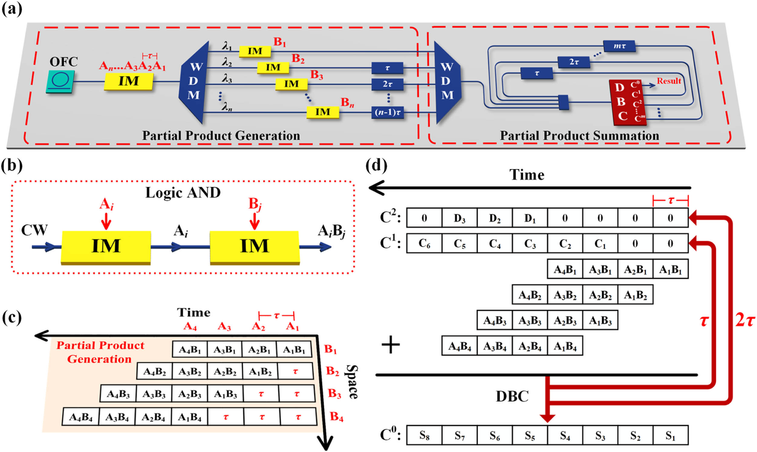
Fig. 1. Principle of the time-space multiplexed photonic-electronic digital multiplier. (a) Schematic of the proposed multiplier architecture. (b) Logic AND operation realized by two cascading IMs. (c) The generated partial products of 4 × 4
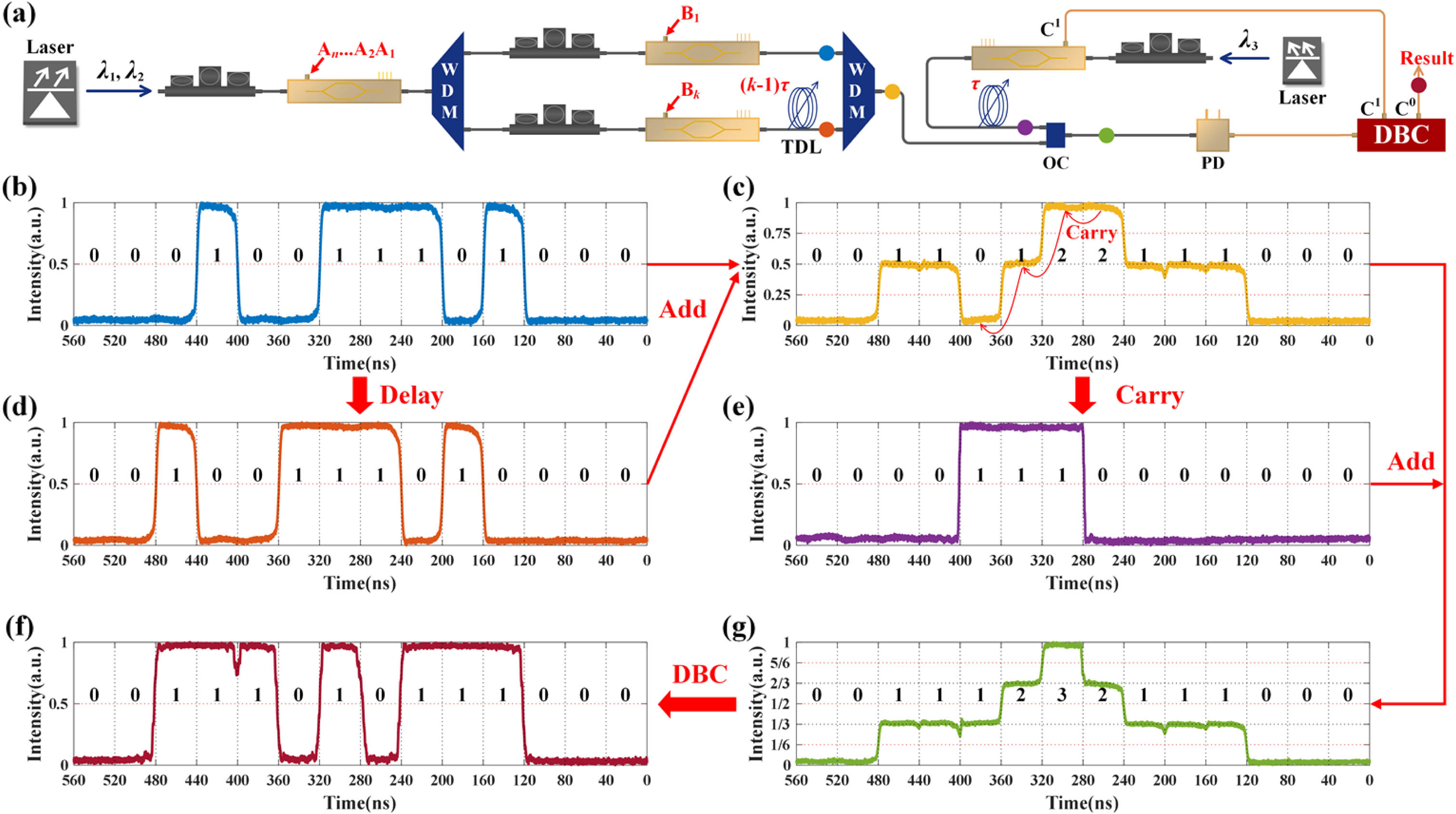
Fig. 2. Experimental results of the 8 × 2 10,011,101 × 11 B 1 B 2 C 1 C 0
Fig. 3. Experimental results of the photonic-electronic digital multiplier with an input operand of 32 bits. (a) and (b) Multiplication results between a 32-bit binary number A 32 … A 2 A 1
Fig. 4. One-step multi-bit DBC realized by the OEO method. (a) Sketch map of multi-bit DBC. (b) The input signal’s state and the corresponding output current level of the PD. (c) Transmission spectrum of the MRR’s drop port under different input signal levels and the input wavelengths.
Fig. 5. Integration scheme of the time-space multiplexed photonic-electronic digital multiplier. (a) Step-by-step summation of the partial products. (b) Schematic diagram of the on-chip photonic-electronic digital multiplier. FPGA, field programmable gate array.

Set citation alerts for the article
Please enter your email address
© Copyright 2018-2021 | Chinese Laser Press. All Rights Reserved 沪ICP备15018463号-20