【AIGC One Sentence Reading】:The study presents a time-space multiplexed design for large-scale photonic-electronic digital multiplication, demonstrating its extensibility and potential for on-chip implementation, paving the way for photonic digital computing.
【AIGC Short Abstract】:This study presents a novel time-space multiplexed architecture for large-scale photonic-electronic digital multiplication, overcoming the limitations of optical nonlinearity. An 8x2-bit multiplier is experimentally demonstrated, showing extensibility and functionality with a 32-bit multiplication at 25 Mbit/s. The architecture also shows potential for on-chip integration, paving the way for large-scale photonic digital computing.
Note: This section is automatically generated by AI . The website and platform operators shall not be liable for any commercial or legal consequences arising from your use of AI generated content on this website. Please be aware of this.
Abstract
Optical computing has shown immense application prospects in the post-Moore era. However, as a crucial component of logic computing, the digital multiplier can only be realized on a small scale in optics, restrained by the limited functionalities and inevitable loss of optical nonlinearity. In this paper, we propose a time-space multiplexed architecture to realize large-scale photonic-electronic digital multiplication. We experimentally demonstrate an -bit photonic-electronic digital multiplier, and the multiplication with a 32-bit number is further executed at 25 Mbit/s to demonstrate its extensibility and functionality. Moreover, the proposed architecture has the potential for on-chip implementation, and a feasible integration scheme is provided. We believe the time-space multiplexed photonic-electronic digital multiplier will open up a promising avenue for large-scale photonic digital computing.
1. INTRODUCTION
Amidst the fast-paced growth of the artificial intelligence and communication industry, the demand for computing resources has surged dramatically. Traditional electronic hardware gradually exhibits the great constraint in accommodating these escalating computing requirements, primarily due to the electronic natural limits of signal processing speed, parallel capacity, and power consumption. To alleviate this bottleneck, photonic computing has emerged as a promising solution, which provides the fast speed for signal processing, multiple dimensions for multiplexing (wavelength, mode, polarization, etc.), and high energy efficiency for data processing [1–4].
Photonic computing can be categorized into two domains: photonic analog computing [5–7] and photonic digital computing [8–10]. Despite impressive breakthroughs in photonic analog computing, it still struggles to excel in high-precision computational scenarios. The analog computing nature along with the noise from optical circuits and the surrounding environment leads to relatively high inaccuracy of results, severely impacting the computing performance and efficiency [11]. In contrast, photonic digital computing offers higher noise tolerance and compatibility with common electronic computer architecture. However, most existing works can only support some simple logic functions such as AND, XOR operations [12–15], one or two-bit adders [16,17], comparators [18–20], and multipliers [21–23]. The limitations of optical nonlinear functionalities and inevitable loss reveal great challenges to execute large-scale digital computing like addition and multiplication. Recently, a feasible way has been proposed to realize a scalable adder based on photonic-electronic computing architecture [24]. As for the multiplier, a large-bit-width computing architecture still remains null.
In this paper, we present a scalable photonic-electronic digital multiplier based on the time-space multiplexed strategy. The two input operands are encoded in time and space dimensions, respectively. By cascading intensity modulators (IMs) to perform AND operation, we obtain the partial products between two operands while loading signals, and then combine them with corresponding delays, thereby achieving the intensity superposition. The mixed signal is then input into the decimal to binary converter (DBC), whose high-bit outputs are delayed by optical waveguides and fed back into the mixed signal to perform the carry propagation, and lowest-bit output is the final result of the multiplier. We design a proof-of-concept experiment to demonstrate the proposed scheme using an electronic analog to digital converter (ADC) instead of the DBC. The -bit photonic-electronic digital multiplier and the multiplication with a 32-bit number are experimentally executed at 25 Mbit/s to demonstrate its extensibility and functionality. There are also potential optical ways to implement the DBC, such as the photonic crystal ADC [25–27] and the optical-electrical-optical (OEO) method mentioned in the discussion section. In addition, an -bit photonic-electronic multiplier architecture is discussed, which can be integrated on a single photonic chip. The proposed method provides a novel paradigm for the optical digital multiplier and explores new opportunities for large-scale photonic logic computing architecture.
Sign up for Photonics Research TOC. Get the latest issue of Photonics Research delivered right to you!Sign up now
2. PRINCIPLE
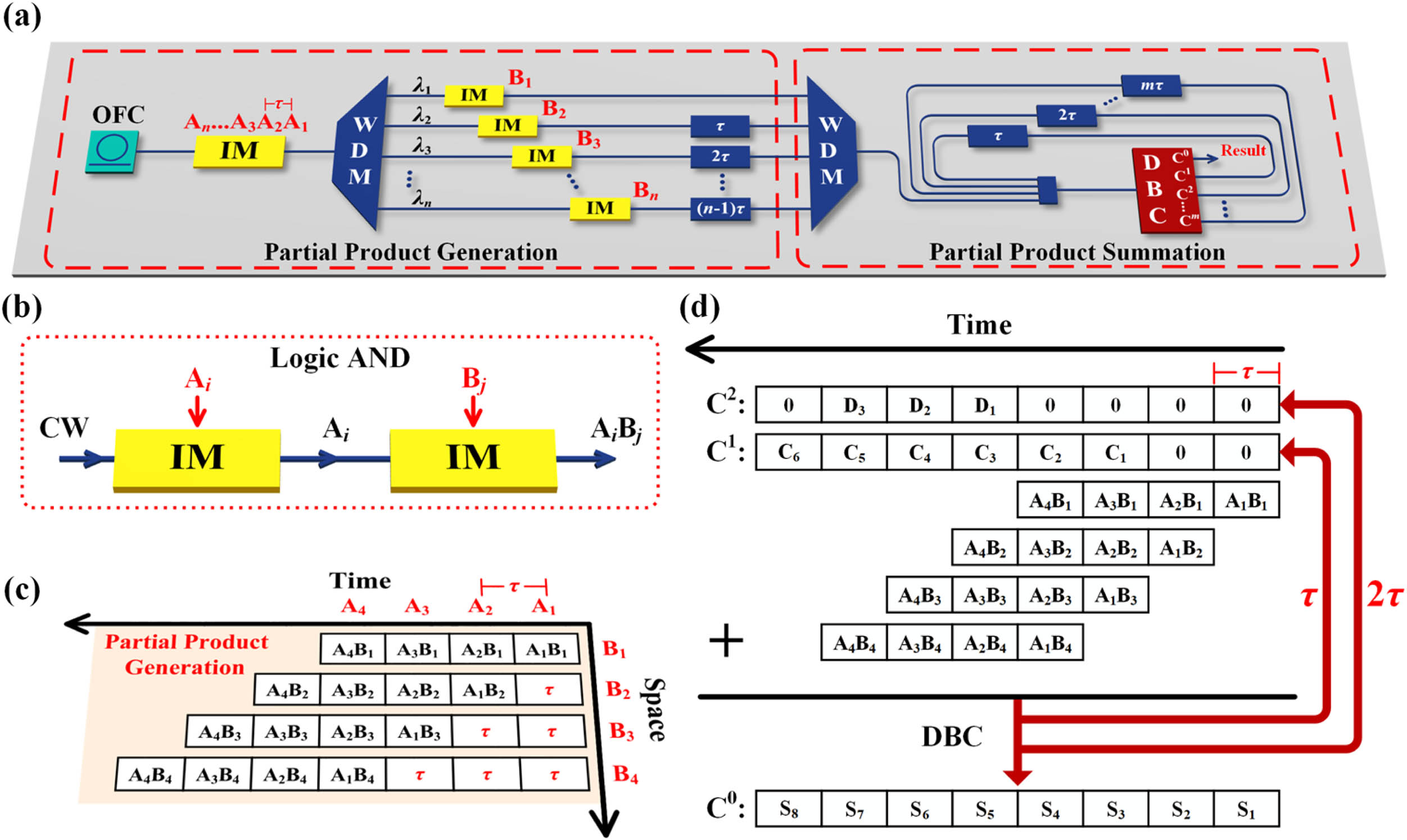
Typically, the multiplication procedure can be divided into two steps: partial product generation and summation. Figure 1(a) depicts the architecture of the time-space multiplexed photonic-electronic digital multiplier. Considering the current optical frequency comb (OFC) technique has been widely applied in photonic systems with a sufficient number of wavelengths and stable working state [28–30], it can serve as a multi-wavelength light source to provide required wavelengths for the multiplier. We encode two input operands in time and space dimensions, respectively. The input operand A () is loaded in a sequence of timestamps whose period equals . The total number of timestamps corresponds to the bit width of the operand A. And each bit of the input operand B () is loaded in different wavelengths () by individual IMs with the duration time of . To generate the partial products, logic AND operation between two input operands is necessary. The cascading IMs shown in Fig. 1(b) provide a favorable way to execute logic AND while loading signals. Only when both input signals are Logic 1, the output optical signal can be Logic 1, corresponding to the AND operation between and . Figure 1(c) depicts the generated partial products of -bit multiplication unfolded in time and space dimensions. Here, we treat the time delay of signals as a form of carry. The time delay of is introduced to achieve the targeted carry for partial products related to . By multiplexing the time and space dimensions, the number of required IMs is linearly related to the bit width of the multiplier, greatly enhancing its scalability.
Figure 1.Principle of the time-space multiplexed photonic-electronic digital multiplier. (a) Schematic of the proposed multiplier architecture. (b) Logic AND operation realized by two cascading IMs. (c) The generated partial products of -bit multiplication unfolded in the dimensions of time and space. (d) The summation procedure of the generated partial products. OFC, optical frequency comb; IM, intensity modulator; WDM, wavelength division multiplexer; DBC, decimal to binary converter; CW, continuous wave.
Having generated the partial products, a wavelength division multiplexer (WDM) is utilized to combine them together. Note that we adopt the WDMs to demultiplex and multiplex multiple wavelengths instead of the multimode interferometer to avoid the coherent superposition of the optical signals. The mixed signal is then input into a DBC, which can convert the multi-level signal into the binary form . Except for the lowest bit, all remaining channels of DBC are looped back as carry signals into the mixed signal. The th-bit output undergoes a time delay of . And the number of carry signals satisfies the following relationship with the bit width of the multiplier:
Figure 1(d) shows the summation procedure of the generated partial products. The DBC’s outputs are mixed with the partial products after corresponding time delays to realize carry propagation. By this means, the lowest bit output of DBC can directly serve as the final bitstream of the multiplier.
3. RESULTS
To validate the proposed principle, a proof-of-concept experiment is implemented as shown in Fig. 2(a). Constrained by the inevitable optical fibers and radio frequency cables to connect all the discrete components, the minimum time delay cannot be reduced to support a high-speed data stream. As a result, we decide to set the multiplication speed at 25Mbit/s. The -bit multiplication is first demonstrated. The input operand of 8 bits is encoded in the time dimension, and the operand of 2 bits is encoded in the space dimension. We load input signals by IMs (Fijitsu H74M-5210-J128), whose bandwidth is 10 GHz and static extinction ratio is 32 dB. Two wavelengths (1549.3 nm) and (1550.1 nm) are utilized to generate the partial products. Figures 2(b) and 2(d) show the generated partial products related to and , respectively. The time delay of the tunable delay line (TDL) determines the bit width of operand and is set to delay here. The TDL is composed of several optic fiber patch cords with a minimum length of 0.1 m. By controlling the total length of fibers, we can adjust the TDL to the desired delay. After the generation of partial products in the optical domain, a WDM is followed to combine them together and outputs the mixed signal as depicted in Fig. 2(c). For the summation part, the input signal of the DBC has at most four levels (0, 1, 2, 3) in the -bit multiplication. Hence a 2-bit DBC is adequate for the task of binarizing the signal. We utilize an electronic ADC to perform the function of 2-bit DBC by quantizing the input signal. Since the ADC’s minimum input voltage is about 5 mV, a bias-tee is used to provide the bias voltage for the electronic signal from PD. The decision voltage interval of the ADC is about 20 mV, which means the ADC will output 00 () when the input voltage is between 5 mV and 25 mV and output 11 when the input voltage is between 65 mV and 85 mV. According to these decision voltage levels, we control the light intensity in each optical channel and the bias voltage of the bias-tee so that the ADC responds accurately to the PD’s output signal with different levels. The voltages of ADC’s input signals are adjusted to about 15 mV, 35 mV, 55 mV, 75 mV corresponding to four input levels 0, 1, 2, 3, and ADC’s output ports will output 00, 01, 10, 11 under these four input voltages, respectively. The output voltage of the ADC is 500 mV, which cannot drive the IM directly. Therefore, we add a microwave amplifier to enable the signal from the output port to drive the IM, thereby converting the electronic carry information into light information. We combine the carry signal with a time delay of [shown in Fig. 2(e)] and the mixed partial products together by an optical coupler to realize the carry propagation. The final optical signal [Fig. 2(g)] is fed into the DBC through a PD to obtain final results of the multiplication from the output port [Fig. 2(g)], which is consistent with the theoretical calculation .
Figure 2.Experimental results of the -bit multiplication for at 25 Mbit/s. (a) Experimental setup to realize photonic-electronic digital multiplier. The circles in the diagram represent the waveforms with the same color detected at those points. (b) and (d) Waveforms of generated partial products related to and , respectively. (c) Waveform of the mixed signals after WDM. (e) and (f) Waveforms of the DBC’s output ports and , respectively. (g) Waveform of the combination between partial products and carry by OC. OC, optical coupler; TDL, tunable delay line; PD, photodetector.
We further expand the multiplier’s scale in the time dimension. By increasing the encoding length of A, the setup can perform the multiplication with an input operand of 32 bits. Figures 3(a) and 3(b) present the results of two -bit multiplication operations. The 32-bit operand can cover nearly numbers, greatly increasing the application range of photonic digital multipliers. And it is quite easy to achieve a larger bit width of operand A, which only needs to encode a longer signal in the time dimension. Moreover, we can change the bit width of operand B by extending the time delays of the generated partial products. As shown in Figs. 3(c) and 3(d), a 32-bit binary number is multiplied by a 3-bit binary number of 101 and a 4-bit binary number of 1001, where the corresponding time delay is set to and , respectively.
Figure 3.Experimental results of the photonic-electronic digital multiplier with an input operand of 32 bits. (a) and (b) Multiplication results between a 32-bit binary number and a 2-bit binary number 11. (c) Multiplication results between a 32-bit binary number and a 3-bit binary number 101. (d) Multiplication results between a 32-bit binary number and a 4-bit binary number 1001.
As the OEO method has been widely used in both optical analog computing and digital computing [31–34], we propose a feasible way to realize one-step multi-bit DBC shown in Fig. 4(a) by the OEO method. The input optical signal of the ()-bit DBC has intensity levels, following the relationship by which will drive the PD to output different electric current levels depicted in Fig. 4(b). The electronic signal will change the position of the microring resonator’s (MRR’s) resonance peak. We can input the wavelengths at corresponding resonance peak positions shown in Fig. 4(c) and use wavelength filters to obtain the desired wavelengths from the drop port of MRR. Take the example of a 2-bit DBC. For the output port , it needs to output light when the input signal is at Level 2 (10) or Level 3 (11). Therefore, the wavelengths at those resonance peak positions (Level 2 and Level 3) will be filtered out. Similarly, for the output port , it will output the wavelengths corresponding to Level 1 (01) and Level 3 (11). The scale of the proposed OEO DBC depends on the number of wavelengths the MRR supports to modulate, which is mainly affected by the following factors. First, the free spectrum range (FSR) of the MRR constrains the wavelength range the DBC can contain. It is preferred to design the MRR with a small radius for large FSR. Second, the MRR’s factor influences the minimum interval of DBC’s input wavelengths. The sharper the MRR’s resonance peak is, the smaller wavelengths’ interval can be set to guarantee the satisfactory extinction ratio of DBC’s output port, which will allow for more wavelengths within a certain wavelength range. Third, the transimpedance amplification capability of MRR’s drive circuit determines the moving range of MRR’s resonance peak. The light current from the PD is required to be amplified and converted into voltage signal, thereby modulating the MRR. To make the MRR’s resonance peak move further, the drive circuit needs to output the signals with higher voltage.
Figure 4.One-step multi-bit DBC realized by the OEO method. (a) Sketch map of multi-bit DBC. (b) The input signal’s state and the corresponding output current level of the PD. (c) Transmission spectrum of the MRR’s drop port under different input signal levels and the input wavelengths.
The implementation of DBC can be also simplified by employing a step-by-step summation method to calculate the sum of partial products. Figure 5(a) shows the procedure involving summations of two addends, which needs 2-bit DBCs and avoids the use of multi-bit DBC. Figure 5(b) presents the schematic diagram of the on-chip photonic-electronic digital multiplier. We can utilize two independent MRRs to execute the function of DBC’s output ports and , respectively. The desired outputs are realized via controlling input wavelengths of MRRs. By this means, the wavelength filter can be omitted. Despite the increase of delay lines and PDs, the step-by-step summation method can reduce the requirements for the design of DBC compared with the one-step DBC, which will make the realization of the photonic-electronic digital multiplier more feasible. Considering signal A needs to be loaded at different wavelengths simultaneously, the corresponding IM can be implemented with the on-chip Mach–Zehnder modulator (MZM) [35–37], which supports parallel modulation of multiple wavelengths. As for signal B, each bit is modulated at one independent wavelength. To achieve more compact integration, we can select the high speed MRRs to load signal B [38–40]. The integrated WDM can be realized by the on-chip arrayed waveguide grating (AWG) [41–43]. And the time delay can be introduced by the on-chip delay lines [44,45]. The integrated structure shortens the feedback time for carry signals, enabling a higher computing speed of the proposed multiplier. Here, we give an area estimation of an -bit digital multiplier of 10 Gbit/s, which includes one MZM (), one eight-channel AWG (), eight MRRs (), all delay lines (), eight PDs (), and seven 2-bit DBCs with corresponding drive circuit (). Assuming the above components account for about 70% of the total area, the multiplier chip will occupy an area of . We can utilize an external field programmable gate array (FPGA) circuit to load signals and obtain computation results while maintaining the chip’s operational state. The OEO scheme of the 2-bit DBC alleviates the impact of optical transmission loss within the chip, making it possible to realize large-scale multipliers.
Figure 5.Integration scheme of the time-space multiplexed photonic-electronic digital multiplier. (a) Step-by-step summation of the partial products. (b) Schematic diagram of the on-chip photonic-electronic digital multiplier. FPGA, field programmable gate array.
In conclusion, we propose a time-space multiplexed multiplier architecture capable of performing large-scale digital multiplication. By encoding the two input operands in the time and space dimensions, the required components are linearly related to the bit width of the multiplier. We experimentally implement a photonic-electronic multiplier to compute the results of an -bit input at 25 Mbit/s. And the multiplication with a 32-bit number is further demonstrated to verify its capability of performing large-scale computations. We also provide two integration schemes with one-step summation and step-by-step summation methods, respectively. The proposed multiplier greatly expands the scale of existing photonic digital multiplication and paves the way for the large-scale optical digital computing.
[15] K. Goswami, H. Mondal, P. Das. Realization of ultra-compact all-optical logic AND Gate based on photonic crystal waveguide. Advances in Communication, Devices and Networking: Proceedings of ICCDN, 61-68(2022).
 AI Video Guide
  AI Picture Guide
 AI One Sentence