
Yanqiu Li, Yan Liu, Lihui Liu. Effect of Thermal Deformation on Imaging Performance for 16 nm Extreme Ultraviolet Lithography Objective[J]. Acta Optica Sinica, 2019, 39(1): 0122001
- Acta Optica Sinica
- Vol. 39, Issue 1, 0122001 (2019)
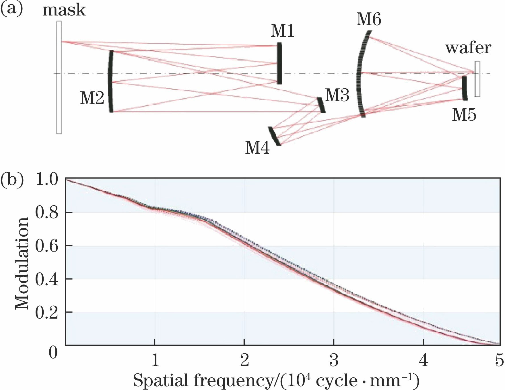
Fig. 1. (a) Layout of EUVL objective; (b) modulation transfer function
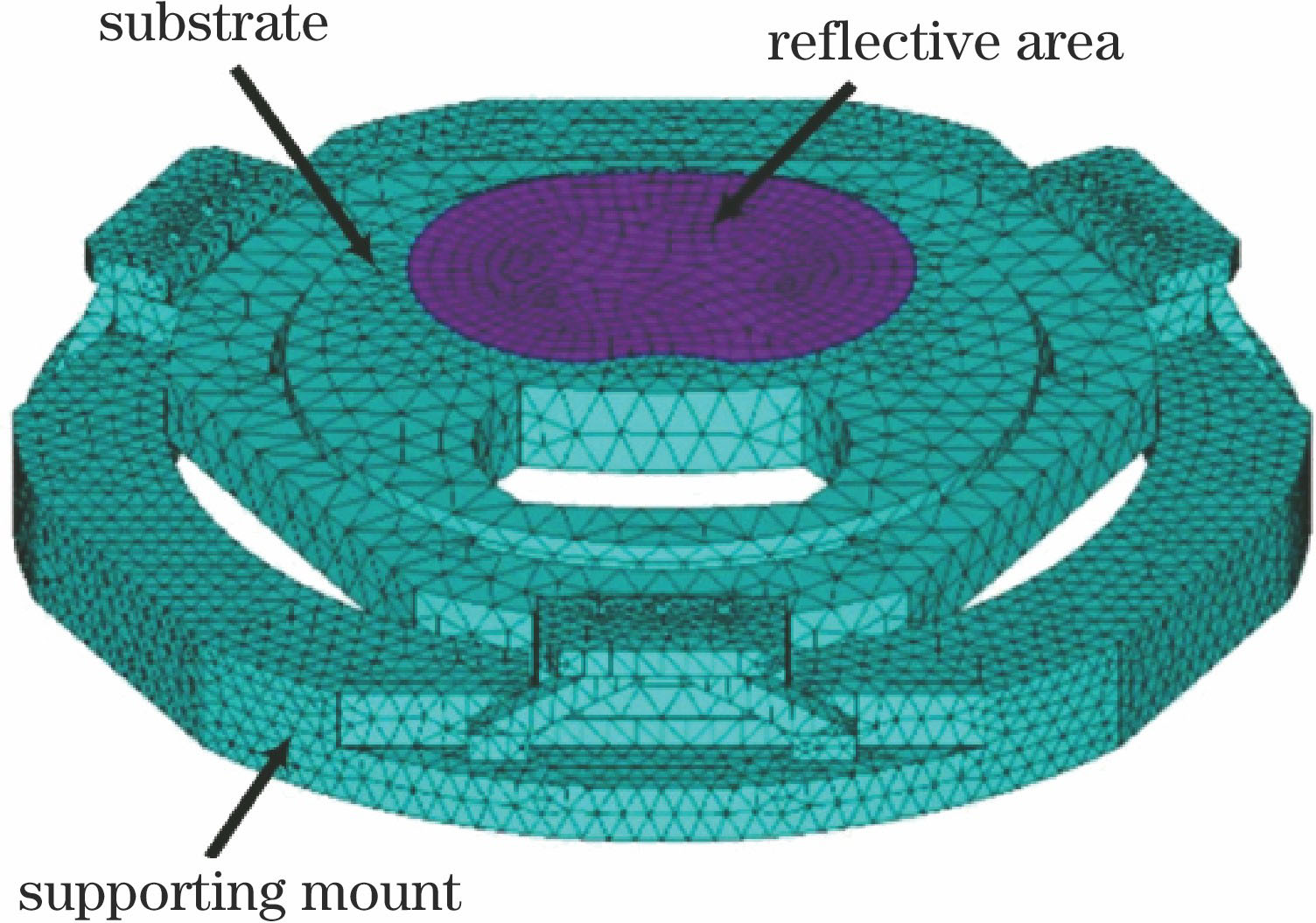
Fig. 2. Finite element model of M1 mirror
Fig. 3. Heat loading steps-time plot of mirror
Fig. 4. (a) Annular distribution of luminous intensity; (b) distribution of illuminance on mask
Fig. 5. Curve of reflectivity of Mo/Si multilayer relative to incidence angle
Fig. 6. (a) Temperature and (b) thermal deformation maps of M1 mirror at the end of last-heat-loading step
Fig. 7. Curves of (a) temperature and (b) thermal deformation RMS value of each mirror relative to time
Fig. 8. Image annular field of view
Fig. 9. (a) WFE RMS and (b) distortion of objective system on the moments of maximum temperature and minimal temperature
Fig. 10. (a) WFE RMS and (b) distortion of edge image field of view caused by thermal deformation of each mirror on maximum temperature moment
Fig. 11. Curvature of each mirror, height of chief ray and incidence angle of chief ray
|
Table 1. Characteristic parameters of mirrors and supporting mount materials
|
Table 2. Model of 16 nm EUVL prototype productivity
|
Table 3. Relevant calculating data of the absorbed EUV power density for each mirror
|
Table 4. Imaging performance demands for objective
|
Table 5. Analysis of thermal deformation for 16 nm and 22 nm EUVL objectives

Set citation alerts for the article
Please enter your email address
© Copyright 2018-2021 | Chinese Laser Press. All Rights Reserved 沪ICP备15018463号-20