• Photonics Research
  • Vol. 10, Issue 9, 2008 (2022)
Xuan Cong1, Hongxin Zeng1, Shiqi Wang1, Qiwu Shi2, Shixiong Liang3, Jiandong Sun4, Sen Gong1、2, Feng Lan1、5, Ziqiang Yang1、5, and Yaxin Zhang1、5、*
Author Affiliations
  • 1Terahertz Science and Technology Research Center, University of Electronic Science and Technology of China, Chengdu 610000, China
  • 2College of Materials Science and Engineering, Sichuan University, Chengdu 610065, China
  • 3National Key Laboratory of Application Specific Integrated Circuit, Hebei Semiconductor Research Institute, Shijiazhuang 050051, China
  • 4Key Laboratory of Nanodevices and Applications, Suzhou Institute of Nano-Tech and Nano-Bionics (SINANO), Chinese Academy of Sciences, Suzhou 215123, China
  • 5Yangtze Delta Region Institute (HuZhou), University of Electronic Science and Technology of China, Huzhou 313001, China
  • show less
    DOI: 10.1364/PRJ.453496 Cite this Article Set citation alerts
    Xuan Cong, Hongxin Zeng, Shiqi Wang, Qiwu Shi, Shixiong Liang, Jiandong Sun, Sen Gong, Feng Lan, Ziqiang Yang, Yaxin Zhang. Dynamic bifunctional THz metasurface via dual-mode decoupling[J]. Photonics Research, 2022, 10(9): 2008 Copy Citation Text show less
    Schematic diagram of dynamic function switching of THz waves via mode decoupling controlled by external physical field stimulus. When y- (or x-) polarized waves impinge vertically, the reflected waves undergo polarization conversion and produce independent phase shifts in the two modes, achieving different functions.
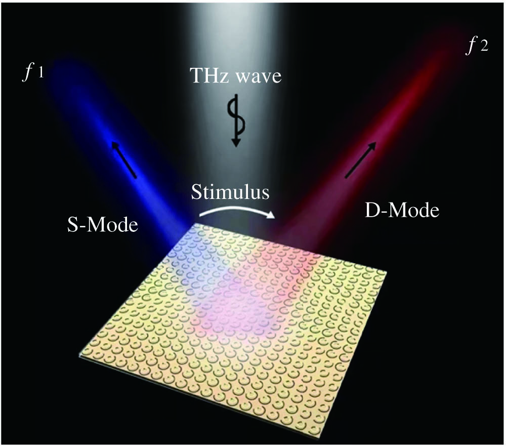
    Fig. 1. Schematic diagram of dynamic function switching of THz waves via mode decoupling controlled by external physical field stimulus. When y- (or x-) polarized waves impinge vertically, the reflected waves undergo polarization conversion and produce independent phase shifts in the two modes, achieving different functions.
    (a) Schematic diagram of the unit structure and parameter annotation. (b) Equivalent structure diagram, (c) surface current distribution, and (d) corresponding S-mode field distribution of the unit in the insulating state at normal temperature. (e) Equivalent structure diagram, (f) surface current distribution, and (g) corresponding D-mode field distribution of the unit in the metallic state at high temperature.
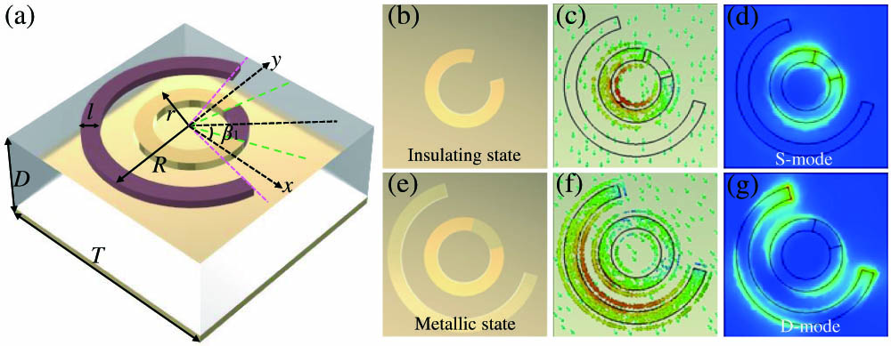
    Fig. 2. (a) Schematic diagram of the unit structure and parameter annotation. (b) Equivalent structure diagram, (c) surface current distribution, and (d) corresponding S-mode field distribution of the unit in the insulating state at normal temperature. (e) Equivalent structure diagram, (f) surface current distribution, and (g) corresponding D-mode field distribution of the unit in the metallic state at high temperature.
    (a) Amplitude of reflected cross-polarization wave in S-mode at room temperature and (b) corresponding phase delay. (c) Amplitude of reflected cross-polarization wave in high-temperature D-mode and (d) corresponding phase delay.
    Fig. 3. (a) Amplitude of reflected cross-polarization wave in S-mode at room temperature and (b) corresponding phase delay. (c) Amplitude of reflected cross-polarization wave in high-temperature D-mode and (d) corresponding phase delay.
    (a) Spectra of the reflected cross-polarized wave (top) and corresponding phase delay (bottom) for forward illuminated y-polarized light in S-mode. (b) Spectra of the reflected cross-polarized wave (top) and corresponding phase delay (bottom) for forward illuminated y-polarized light in D-mode. Amplitude–phase distribution of reflected cross-polarization at 340 GHz for the selected superatom in (c) S-mode and (d) D-mode.
    Fig. 4. (a) Spectra of the reflected cross-polarized wave (top) and corresponding phase delay (bottom) for forward illuminated y-polarized light in S-mode. (b) Spectra of the reflected cross-polarized wave (top) and corresponding phase delay (bottom) for forward illuminated y-polarized light in D-mode. Amplitude–phase distribution of reflected cross-polarization at 340 GHz for the selected superatom in (c) S-mode and (d) D-mode.
    Simulation and experimental results of the reflected cross-polarized wave focusing off-axis with tunable focal length when y-polarized wave is vertically incident. (a) Simulation results of Ex distribution in xoz plane in S-mode. (b) Simulation results of Ex distribution in xoz plane in D-mode. (c)–(e) Experimental results of Ix distribution measured at sections A (L=15 mm), B (L=17 mm), and C (L=20 mm) in (a). (f)–(h) Experimental results of Ix distribution measured at sections D (L=11 mm), E (L=13 mm), and F (L=15 mm) in (b).
    Fig. 5. Simulation and experimental results of the reflected cross-polarized wave focusing off-axis with tunable focal length when y-polarized wave is vertically incident. (a) Simulation results of Ex distribution in xoz plane in S-mode. (b) Simulation results of Ex distribution in xoz plane in D-mode. (c)–(e) Experimental results of Ix distribution measured at sections A (L=15  mm), B (L=17  mm), and C (L=20  mm) in (a). (f)–(h) Experimental results of Ix distribution measured at sections D (L=11  mm), E (L=13  mm), and F (L=15  mm) in (b).
    Simulation and experimental results of the reflected cross-polarized wave focusing off-axis with large-angle focus deflection when y-polarized wave is vertically incident. (a) Simulation results of Ex distribution in xoz plane in S-mode. (b) Simulation results of Ex distribution in xoz plane in D-mode. (c)–(e) Experimental results of Ix distribution measured at sections A (L=11 mm), B (L=13 mm), and C (L=15 mm) in (a). (f)–(h) Experimental results of Ix distribution measured at sections D (L=11 mm), E (L=13 mm), and F (L=15 mm) in (b).
    Fig. 6. Simulation and experimental results of the reflected cross-polarized wave focusing off-axis with large-angle focus deflection when y-polarized wave is vertically incident. (a) Simulation results of Ex distribution in xoz plane in S-mode. (b) Simulation results of Ex distribution in xoz plane in D-mode. (c)–(e) Experimental results of Ix distribution measured at sections A (L=11  mm), B (L=13  mm), and C (L=15  mm) in (a). (f)–(h) Experimental results of Ix distribution measured at sections D (L=11  mm), E (L=13  mm), and F (L=15  mm) in (b).
    (a) Image of a fabricated metasurface sample and (b) its partially enlarged view. (c) Schematic diagram of the experimental setup.
    Fig. 7. (a) Image of a fabricated metasurface sample and (b) its partially enlarged view. (c) Schematic diagram of the experimental setup.
    Xuan Cong, Hongxin Zeng, Shiqi Wang, Qiwu Shi, Shixiong Liang, Jiandong Sun, Sen Gong, Feng Lan, Ziqiang Yang, Yaxin Zhang. Dynamic bifunctional THz metasurface via dual-mode decoupling[J]. Photonics Research, 2022, 10(9): 2008
    Download Citation