• Acta Optica Sinica
  • Vol. 44, Issue 5, 0504001 (2024)
Juan Zhang, Er Yao, and Shaoying Ke*
Author Affiliations
  • Key Laboratory of Light Field Manipulation and System Integration Applications in Fujian Province, College of Physics and Information Engineering, Minnan Normal University, Zhangzhou 363000, Fujian , China
  • show less
    DOI: 10.3788/AOS231693 Cite this Article Set citation alerts
    Juan Zhang, Er Yao, Shaoying Ke. Optimal Design of Charge-Free Layer InGaAs/Si Avalanche Photodetector[J]. Acta Optica Sinica, 2024, 44(5): 0504001 Copy Citation Text show less
    3D structural diagram of charge-free layer InGaAs/Si APD
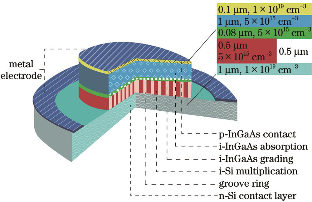
    Fig. 1. 3D structural diagram of charge-free layer InGaAs/Si APD
    Effect of different dielectric materials in the grooved ring on the charge-free layer InGaAs/Si APD. (a) Current; (b) current at 95%Vb; (c) avalanche voltage
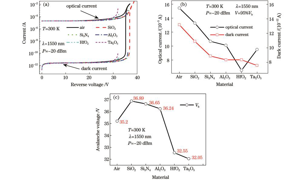
    Fig. 2. Effect of different dielectric materials in the grooved ring on the charge-free layer InGaAs/Si APD. (a) Current; (b) current at 95%Vb; (c) avalanche voltage
    Changes of recombination rate of charge-free layer InGaAs/Si APD with media. (a) Section diagram of recombination rate structure; (b) recombination rate curves taken at X=16.229
    Fig. 3. Changes of recombination rate of charge-free layer InGaAs/Si APD with media. (a) Section diagram of recombination rate structure; (b) recombination rate curves taken at X=16.229
    Changes of electron and hole concentrations of charge-free layer InGaAs/Si APD with media. (a) Electron concentration in structural section; (b) hole concentration in structural section; (c) electron concentration at X=16.229; (d) hole concentration at X=16.229
    Fig. 4. Changes of electron and hole concentrations of charge-free layer InGaAs/Si APD with media. (a) Electron concentration in structural section; (b) hole concentration in structural section; (c) electron concentration at X=16.229; (d) hole concentration at X=16.229
    Effect of different dielectric materials in the grooved ring on the charge-free layer InGaAs/Si APD. (a) Conduction band of bonding interface; (b) valence band of bonding interface; (c) charge concentration
    Fig. 5. Effect of different dielectric materials in the grooved ring on the charge-free layer InGaAs/Si APD. (a) Conduction band of bonding interface; (b) valence band of bonding interface; (c) charge concentration
    Effect of different dielectric materials in the grooved ring on the charge-free layer InGaAs/Si APD. (a) Impact ionization rate (RIIR) of structural section; (b) impact ionization rate at X=16.229; (c) electron ionization coefficient at X=16.229; (d) hole ionization coefficient at X=16.229
    Fig. 6. Effect of different dielectric materials in the grooved ring on the charge-free layer InGaAs/Si APD. (a) Impact ionization rate (RIIR) of structural section; (b) impact ionization rate at X=16.229; (c) electron ionization coefficient at X=16.229; (d) hole ionization coefficient at X=16.229
    Variation of electric field in the charge-free layer InGaAs/Si APD with media. (a) Electric field of structural section; (b) electric field at X=16.229
    Fig. 7. Variation of electric field in the charge-free layer InGaAs/Si APD with media. (a) Electric field of structural section; (b) electric field at X=16.229
    Variation of InGaAs/Si APD gain with media. (a) Gain curves; (b) gain at 95%Vb
    Fig. 8. Variation of InGaAs/Si APD gain with media. (a) Gain curves; (b) gain at 95%Vb
    3 dB bandwidth curves of InGaAs/Si APD without charge layer
    Fig. 9. 3 dB bandwidth curves of InGaAs/Si APD without charge layer
    Variation of electron and hole rates in the charge-free layer InGaAs/Si APD at X=16.229 with media. (a) Electron rate; (b) hole rate
    Fig. 10. Variation of electron and hole rates in the charge-free layer InGaAs/Si APD at X=16.229 with media. (a) Electron rate; (b) hole rate
    Gain-bandwidth product of charge-free layer InGaAs/Si APD
    Fig. 11. Gain-bandwidth product of charge-free layer InGaAs/Si APD
    Serial numberMaterialDielectric constant
    1Air1.0
    2SiO23.9
    3Si3N47.5
    4Al2O39.3
    5HfO222.0
    6Ta2O526.0
    Table 1. Parameters of groove ring filling materials
    Juan Zhang, Er Yao, Shaoying Ke. Optimal Design of Charge-Free Layer InGaAs/Si Avalanche Photodetector[J]. Acta Optica Sinica, 2024, 44(5): 0504001
    Download Citation