• Photonics Research
  • Vol. 8, Issue 11, 1786 (2020)
F. Piva1、*, C. De Santi1, M. Deki2, M. Kushimoto2, H. Amano2, H. Tomozawa3, N. Shibata3, G. Meneghesso1, E. Zanoni1, and M. Meneghini1
Author Affiliations
  • 1Department of Information Engineering, University of Padova, Padova, Italy
  • 2Institute of Materials and Systems for Sustainability (IMaSS), Nagoya University, Nagoya 464-8601, Japan
  • 3Nikkiso Giken Co., Ltd., 1-5-1 Asahigaoka, Hakusan, Ishikawa 924-0004, Japan
  • show less
    DOI: 10.1364/PRJ.401785 Cite this Article Set citation alerts
    F. Piva, C. De Santi, M. Deki, M. Kushimoto, H. Amano, H. Tomozawa, N. Shibata, G. Meneghesso, E. Zanoni, M. Meneghini. Modeling the degradation mechanisms of AlGaN-based UV-C LEDs: from injection efficiency to mid-gap state generation[J]. Photonics Research, 2020, 8(11): 1786 Copy Citation Text show less
    Electrical characterization during the stress, in semi-logarithmic scale, carried out before and during the stress experiment at 250 mA. All measurements were taken at 25°C.
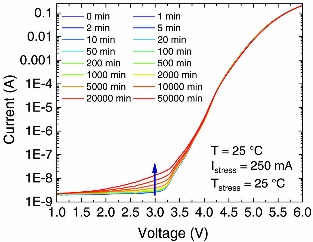
    Fig. 1. Electrical characterization during the stress, in semi-logarithmic scale, carried out before and during the stress experiment at 250 mA. All measurements were taken at 25°C.
    (a) Normalized current at the voltage of 3 V, and (b) normalized series resistance (Rs) at the temperatures of 25°C and 75°C during the stress.
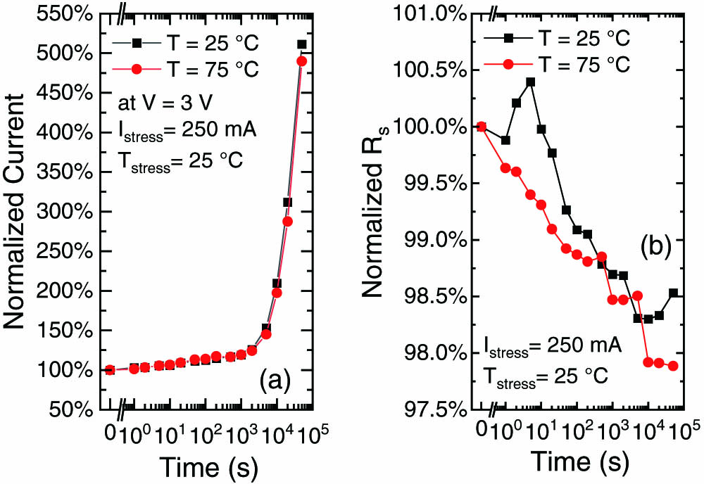
    Fig. 2. (a) Normalized current at the voltage of 3 V, and (b) normalized series resistance (Rs) at the temperatures of 25°C and 75°C during the stress.
    Ideality factor at the temperature of 25°C during the stress.
    Fig. 3. Ideality factor at the temperature of 25°C during the stress.
    (a) Optical power (OP) during the stress at the temperature of 25°C. (b) Normalized optical power at three different current levels: 10 μA, 1 mA, and 100 mA.
    Fig. 4. (a) Optical power (OP) during the stress at the temperature of 25°C. (b) Normalized optical power at three different current levels: 10 μA, 1 mA, and 100 mA.
    Simplified representation of the increase in the injection barrier due to the presence of a distributed negative charge near/within the active region.
    Fig. 5. Simplified representation of the increase in the injection barrier due to the presence of a distributed negative charge near/within the active region.
    Schematic representation of the reactions.
    Fig. 6. Schematic representation of the reactions.
    Optical degradation measured at 25°C and 75°C during stress at 250 mA. Solid lines represent the solution of the system of ODEs reported above, showing a good agreement with the experimental data.
    Fig. 7. Optical degradation measured at 25°C and 75°C during stress at 250 mA. Solid lines represent the solution of the system of ODEs reported above, showing a good agreement with the experimental data.
    Fitting of the optical power data at low current level with the function proposed in Ref. [24].
    Fig. 8. Fitting of the optical power data at low current level with the function proposed in Ref. [24].
    Power spectral density during the aging at the current of 1 mA and at the temperature of 25°C.
    Fig. 9. Power spectral density during the aging at the current of 1 mA and at the temperature of 25°C.
    (a) SSPC measurement during the aging, and (b) correlation between the second defect from SSPC and the optical power at low current levels.
    Fig. 10. (a) SSPC measurement during the aging, and (b) correlation between the second defect from SSPC and the optical power at low current levels.
    F. Piva, C. De Santi, M. Deki, M. Kushimoto, H. Amano, H. Tomozawa, N. Shibata, G. Meneghesso, E. Zanoni, M. Meneghini. Modeling the degradation mechanisms of AlGaN-based UV-C LEDs: from injection efficiency to mid-gap state generation[J]. Photonics Research, 2020, 8(11): 1786
    Download Citation