• Infrared and Laser Engineering
  • Vol. 51, Issue 1, 20210811 (2022)
Junjie Si1、2、3
Author Affiliations
  • 11. China Airborne Missile Academy, Luoyang 471009, China
  • 22. Aviation Key Laboratory of Science and Technology on Infrared Detector, Luoyang 471009, China
  • 33. Henan Antimonide Infrared Detector Engineering Center, Luoyang 471009, China
  • show less
    DOI: 10.3788/IRLA20210811 Cite this Article
    Junjie Si. Novel InSb-based infrared detector materials (Invited)[J]. Infrared and Laser Engineering, 2022, 51(1): 20210811 Copy Citation Text show less
    Crystal structure of InSb
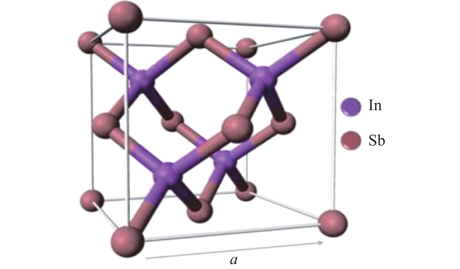
    Fig. 1. Crystal structure of InSb
    Brillouin zone (a) and band structure (b) of InSb crystal (calculated by empirical pseudopotential method without spin-orbit coupling)
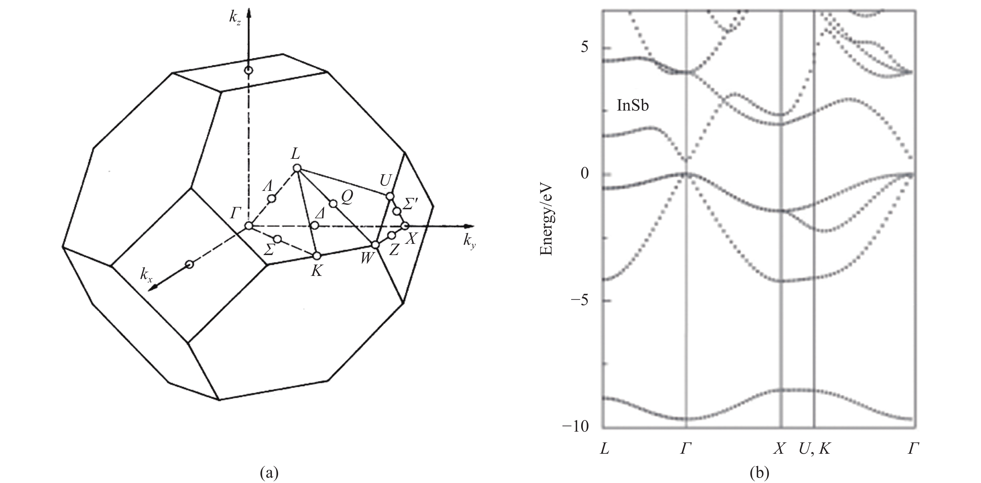
    Fig. 2. Brillouin zone (a) and band structure (b) of InSb crystal (calculated by empirical pseudopotential method without spin-orbit coupling)
    Band gap of energy valley of crystal InSb
    Fig. 3. Band gap of energy valley of crystal InSb
    Band gap of InSb crystal variation with temperature
    Fig. 4. Band gap of InSb crystal variation with temperature
    Fermi level of InSb crystal variation with temperature for different shallow donor or acceptor concentration
    Fig. 5. Fermi level of InSb crystal variation with temperature for different shallow donor or acceptor concentration
    Band gap of some typical compound semiconductors and their corresponding lattice constant
    Fig. 6. Band gap of some typical compound semiconductors and their corresponding lattice constant
    Minimum direct band gap and electron effective mass at Γ-point of In1−xGaxSb alloy variation with GaSb content x
    Fig. 7. Minimum direct band gap and electron effective mass at Γ-point of In1−xGaxSb alloy variation with GaSb content x
    Phase relation in the pseudo-binary system of InSb-GaSb
    Fig. 8. Phase relation in the pseudo-binary system of InSb-GaSb
    Lattice constant of In1−xGaxSb alloy variation with Ga composition
    Fig. 9. Lattice constant of In1−xGaxSb alloy variation with Ga composition
    Band gap of InGaNSb alloy and its lattice constant
    Fig. 10. Band gap of InGaNSb alloy and its lattice constant
    Band gap of In1−xAlxSb alloy variation with Al composition
    Fig. 11. Band gap of In1−xAlxSb alloy variation with Al composition
    320×256 MBE grown InSb (a) and In1−xAlxSb (b) IRFPA dark current distribution (@90 K, −0.168 V bias (a) and −0.183 V bias (b))
    Fig. 12. 320×256 MBE grown InSb (a) and In1−xAlxSb (b) IRFPA dark current distribution (@90 K, −0.168 V bias (a) and −0.183 V bias (b))
    Band gap of InAs1−xSbx alloy variation with Sb compositionx
    Fig. 13. Band gap of InAs1−xSbx alloy variation with Sb compositionx
    Phase relation in the pseudo-binary system of InSb-InAs
    Fig. 14. Phase relation in the pseudo-binary system of InSb-InAs
    Mobility of InAs1−xSbx alloy variation with Sb composition
    Fig. 15. Mobility of InAs1−xSbx alloy variation with Sb composition
    Band gap of quarternary alloy (GaSb)1−z(InAs0.91Sb0.09)z variation with composition z
    Fig. 16. Band gap of quarternary alloy (GaSb)1−z(InAs0.91Sb0.09)z variation with composition z
    Spectral response curve of InBixSb1−xphoto diode
    Fig. 17. Spectral response curve of InBixSb1−xphoto diode
    Band gap of InBi0.04Sb0.96 alloy variation with temperature
    Fig. 18. Band gap of InBi0.04Sb0.96 alloy variation with temperature
    Phase relation in the pseudo-binary material of InSb-TlSb
    Fig. 19. Phase relation in the pseudo-binary material of InSb-TlSb
    Energy band diagram of In1−xTlxSb and Hg1−xCdxTe with 0.1 eV band gap
    Fig. 20. Energy band diagram of In1−xTlxSb and Hg1−xCdxTe with 0.1 eV band gap
    Band gap of In1−xTlxSb alloy variation with Tl composition x
    Fig. 21. Band gap of In1−xTlxSb alloy variation with Tl composition x
    Spectral response curve of In1−xTlxSb photo diode
    Fig. 22. Spectral response curve of In1−xTlxSb photo diode
    Band gap of InNxSb1−x alloy variation with N composition
    Fig. 23. Band gap of InNxSb1−x alloy variation with N composition
    Band gap of InNxSb1−x alloy variation before and after annealing
    Fig. 24. Band gap of InNxSb1−x alloy variation before and after annealing
    Band gap of InSb quantum wire variation with wire diameter
    Fig. 25. Band gap of InSb quantum wire variation with wire diameter
    Photo response curve of InSb quantum wire with infrared light incident frequency under room temperature @1 Hz
    Fig. 26. Photo response curve of InSb quantum wire with infrared light incident frequency under room temperature @1 Hz
    InSb self-assembly QD barrier detector. QD-BIRD structure ( Left), Band diagram of QD-BIRD absorption zone (upper right), Band diagram of InSb QD area in the absorption zone (lower right)
    Fig. 27. InSb self-assembly QD barrier detector. QD-BIRD structure ( Left), Band diagram of QD-BIRD absorption zone (upper right), Band diagram of InSb QD area in the absorption zone (lower right)
    PL spectrum (a) and quantum efficiency at different working temperatures (b) of InSb QD barrier detector
    Fig. 28. PL spectrum (a) and quantum efficiency at different working temperatures (b) of InSb QD barrier detector
    Transmission electron microscope (TEM) photos of InSb colloidal quantum dots (a), high resolution TEM image (b), light absorption spectrum (black line) and photofluorescence spectrum (red line) (c)
    Fig. 29. Transmission electron microscope (TEM) photos of InSb colloidal quantum dots (a), high resolution TEM image (b), light absorption spectrum (black line) and photofluorescence spectrum (red line) (c)
    ParameterT/K ValueUnit
    *: Electron mass in free space, 9.11×10⁻³¹ kg
    Lattice constant3000.64782nm
    Thermal expansion coefficient3005.04×10−6K−1
    776.5×10⁻⁶K−2
    Density3005.775g·cm−3
    Melting pointTm798K
    Specific heat3000.2J·g−1·℃−1
    Thermal diffusivity3000.16cm2·s−1
    Debye temperature220K
    Band gap Eg4.20.2357eV
    770.228eV
    3000.172eV
    Electron effective mass at Γ valley 3000.013m0*
    Heavy hole mass3000.41m0*
    Light hole mass3000.015m0*
    Electron mobility μe77106cm2·V−1·s−1
    3008×10 4cm2·V−1·s−1
    Hole mobility μh77104cm2·V−1·s−1
    3008×10 2cm2·V−1·s−1
    Intrinsic carrier concentration ni772.6×10 9cm−3
    2009.1×1014cm−3
    3001.5×1015cm−3
    Static dielectric constant30016.8
    High frequency dielectric constant30015.7
    Intrinsic resistivity3004.00×10−3Ω·cm
    Refractive index n3004.0@λ =4 μm
    3004.0@λ =7 μm
    Extinction coefficient k3000.11@λ =4 μm
    3000.025@λ =7 μm
    Table 1. Basic characteristic parameter of InSb crystal
    Lattice structure Lattice constant/ nm Band gap Eg/eV Effective mass Mobility/ cm2·V−1·s−1Intrinsic carrier concentration/ cm−3
    Zinc blende 0.6360.138 (4.2 K) 0.136 (80 K) 0.100 (300 K) 0.0101 (me/m0) 0.41 (mh/m0) 5×10⁵ (μe) 5×10⁴ (μh) 2.0×10¹² (77 K) 8.6×10¹⁵ (200 K) 4.1×10¹⁶ (300 K)
    Table 2. Characteristic parameters of InAs0.35Sb0.65
    Junjie Si. Novel InSb-based infrared detector materials (Invited)[J]. Infrared and Laser Engineering, 2022, 51(1): 20210811
    Download Citation