• Photonics Research
  • Vol. 5, Issue 6, B15 (2017)
Zejie Yu, Haoran Cui, and Xiankai Sun*
Author Affiliations
  • Department of Electronic Engineering, The Chinese University of Hong Kong, Shatin, New Territories, Hong Kong SAR, China
  • show less
    DOI: 10.1364/PRJ.5.000B15 Cite this Article Set citation alerts
    Zejie Yu, Haoran Cui, Xiankai Sun. Genetically optimized on-chip wideband ultracompact reflectors and Fabry–Perot cavities[J]. Photonics Research, 2017, 5(6): B15 Copy Citation Text show less
    (a) Initial silicon slab before design optimization. (b) Final optimized structure of the on-chip reflector. Field profiles (Ey component) as the input TE0 mode at a wavelength of 1550 nm reflects (c) from the initial silicon slab and (d) from the optimized structure. Field profiles (Ey component) (e) of the reflected light and (f) of the source at the wavelength of 1550 nm. The scale bars represent 1 μm in (a)–(d) and represent 0.5 μm in (e) and (f). (g) Color code for the vertical structures in (a) and (b). Gray/red pixels denotes the etched/unetched area where no/220-nm silicon layer remains on top of the oxide.
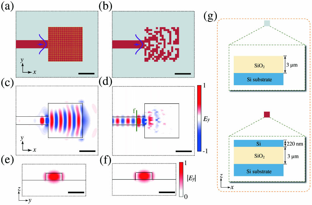
    Fig. 1. (a) Initial silicon slab before design optimization. (b) Final optimized structure of the on-chip reflector. Field profiles (Ey component) as the input TE0 mode at a wavelength of 1550 nm reflects (c) from the initial silicon slab and (d) from the optimized structure. Field profiles (Ey component) (e) of the reflected light and (f) of the source at the wavelength of 1550 nm. The scale bars represent 1 μm in (a)–(d) and represent 0.5 μm in (e) and (f). (g) Color code for the vertical structures in (a) and (b). Gray/red pixels denotes the etched/unetched area where no/220-nm silicon layer remains on top of the oxide.
    (a) Flow chart for the genetic optimization process. (b) Illustration showing the crossover process. (c) Reflectivity spectra of the optimized reflector structure (red solid) and of the initial silicon slab (blue dashed). (d) Illustration showing the corner rounding effect. (e) Reflectivity spectra of the optimized reflector considering the corner rounding effect with different rounding radii.
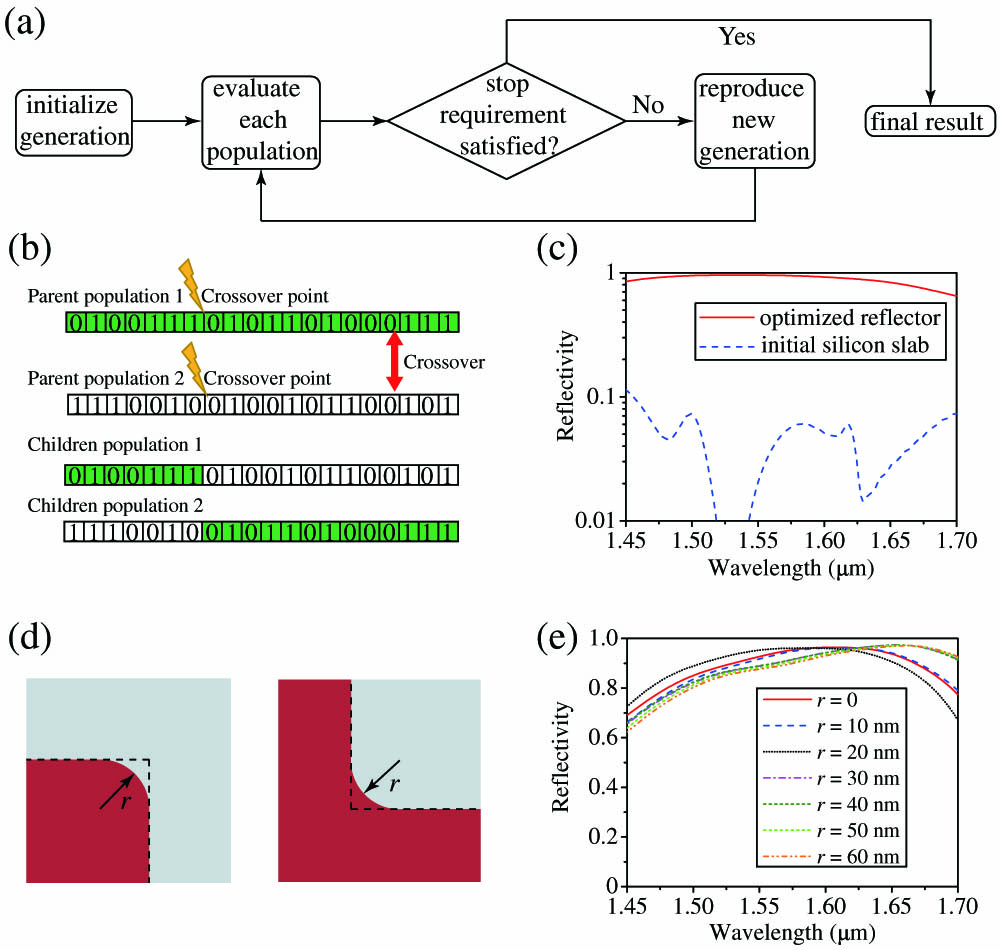
    Fig. 2. (a) Flow chart for the genetic optimization process. (b) Illustration showing the crossover process. (c) Reflectivity spectra of the optimized reflector structure (red solid) and of the initial silicon slab (blue dashed). (d) Illustration showing the corner rounding effect. (e) Reflectivity spectra of the optimized reflector considering the corner rounding effect with different rounding radii.
    (a) Layout of an FP cavity constructed from the optimized reflectors. (b) Calculated normalized transmission spectrum of the FP cavity. (c) Normalized transmission spectrum zoomed in at an optical resonance at ∼1551 nm.
    Fig. 3. (a) Layout of an FP cavity constructed from the optimized reflectors. (b) Calculated normalized transmission spectrum of the FP cavity. (c) Normalized transmission spectrum zoomed in at an optical resonance at 1551  nm.
    (a) Optical microscope image of an FP cavity device. (b) Zoomed-in SEM image of the left grating coupler. (c) Zoomed-in SEM image of the right reflector.
    Fig. 4. (a) Optical microscope image of an FP cavity device. (b) Zoomed-in SEM image of the left grating coupler. (c) Zoomed-in SEM image of the right reflector.
    (a) Normalized transmission spectrum of an FP cavity device. The wide-range spectrum is composed of spectra measured from four devices with identical FP cavities but different grating couplers to cover different wavelength bands. The red dashed lines denote the stitching points of the spectra. Zoomed-in spectra showing optical resonances at (b) 1443 and (c) 1620 nm, each fitted with a Lorentzian resonance line shape (red).
    Fig. 5. (a) Normalized transmission spectrum of an FP cavity device. The wide-range spectrum is composed of spectra measured from four devices with identical FP cavities but different grating couplers to cover different wavelength bands. The red dashed lines denote the stitching points of the spectra. Zoomed-in spectra showing optical resonances at (b) 1443 and (c) 1620 nm, each fitted with a Lorentzian resonance line shape (red).
    Reflectivity spectra of the optimized reflectors simulated for the ideal structure (blue solid line), simulated for the fabricated structure (black dashed line), and derived from the experimentally measured FP cavity quality factors (red dots).
    Fig. 6. Reflectivity spectra of the optimized reflectors simulated for the ideal structure (blue solid line), simulated for the fabricated structure (black dashed line), and derived from the experimentally measured FP cavity quality factors (red dots).
    Zejie Yu, Haoran Cui, Xiankai Sun. Genetically optimized on-chip wideband ultracompact reflectors and Fabry–Perot cavities[J]. Photonics Research, 2017, 5(6): B15
    Download Citation