Abstract
Reflectors are an essential component for on-chip integrated photonics. Here, we propose a new method for designing reflectors on the prevalent thin-film-on-insulator platform by using genetic-algorithm optimization. In simulation, the designed reflector with a footprint of only 2.16 μm×2.16 μm can achieve ~97% reflectivity and 1 dB bandwidth as wide as 220 nm. The structure is composed of randomly distributed pixels and is highly robust against the inevitable corner rounding effect in device fabrication. In experiment, we fabricated on-chip Fabry–Perot (FP) cavities constructed from optimized reflectors. Those FP cavities have intrinsic quality factors of >2000 with the highest value beyond 4000 in a spectral width of 200 nm. The reflectivity fitted from the FP cavity resonances is >85% in the entire wavelength range of 1440–1640 nm and is beyond 95% at some wavelengths. The fabrication processes are CMOS compatible and require only one step of lithography and etch. The devices can be used as a standard module in integrated photonic circuitry for wide applications in on-chip semiconductor laser structures and optical signal processing.1. INTRODUCTION
Thin film on insulator is a popular platform for integrated photonics because it enables research and applications that require strong light confinement and light–matter interaction. Reflectors are one of the most important components in integrated photonics, which serve many functions, such as laser cavities [1–3], filters [4,5], and attenuators [6]. Distributed Bragg reflectors (DBRs) are a type of widely used reflectors. However, they usually require deeply or fully etched grating trenches in thick materials to achieve the high index contrast [5], which is incompatible with the thin-film-on-insulator technology. Some DBRs demonstrated recently have thin-film-on-insulator compatibility [6,7], but they require a large footprint, which is undesirable for high-density on-chip integration. On the other hand, reflectors using cleaved facets of a semiconductor material with high-reflection coatings [8,9] are both thin-film-on-insulator compatible and of compact size. However, they usually require complicated fabrication processes that lead to high cost and low yield. Therefore, a reflector on the thin-film-on-insulator platform with compact size and simple fabrication process is yet to be invented.
Mathematical optimization is a general and robust design tool with wide applications in multidisciplinary areas of science and engineering. Nanophotonic devices designed by mathematical optimization can achieve different functionalities with many advantages, such as low loss, wide band, and ultracompact size [10–14]. Piggott et al. [15] and Shen et al. [16] independently proposed optimization techniques and achieved ultracompact wavelength demultiplexer and polarization demultiplexer, respectively. Recently, many other research groups also demonstrated other functional nanophotonic devices using mathematical optimization. For example, Mak et al. [17] studied 3 dB power splitters making use of the binary particle swarm optimization algorithm. Xu et al. [18] further optimized and experimentally obtained all-passive photonic power dividers with arbitrary power ratios using a nonlinear fast search method. Frellsen et al. [19] designed and experimentally verified low-loss and broadband two-mode (de)multiplexers, which (de)multiplex the fundamental and the first-order transverse-electric modes in a silicon photonic wire.
In this paper, we propose to design reflectors by mathematical optimization with a genetic algorithm. The optimized reflectors have a footprint of only , the smallest demonstrated to date among those that do not rely on additional coatings on the thin-film-on-insulator platform. The simulated reflectivity can be more than 97% and the 1 dB bandwidth is as wide as 220 nm. In addition, the structure is highly robust against the corner rounding effect in device fabrication. Experimentally, we demonstrated Fabry–Perot (FP) cavities by connecting the optimized integrated reflectors with a waveguide. The FP cavities possess intrinsic optical quality factors higher than 2000 in the range of 1440–1640 nm with the highest value beyond 4000. The reflectivity derived from the fitted quality factors of the FP resonances is higher than 85% in 1440–1640 nm and is more than 95% at some cavity resonances. Such genetically optimized integrated reflectors and FP cavities have great significance. First, although the optimized shape cannot be transferred directly to another material platform, the optimization algorithm and design method are generic and can be employed to design reflectors elsewhere. Second, the distance between the two reflectors can be flexibly designed and thus can be as small as an optical wavelength. This could enable single cavity resonance with its free spectral range broader than the material’s gain spectrum width, which cannot be achieved in microring resonators due to the unavoidable bending loss when the ring radius is small [20]. Therefore, such FP cavities realized in active materials may lead to ultracompact single-mode lasers. In addition, the performance (e.g., quality factors) of microring resonators can be enhanced when combined with such FP cavities, which may have wide applications in sensing and telecommunications [21].
Sign up for Photonics Research TOC. Get the latest issue of Photonics Research delivered right to you!Sign up now
2. DESIGN WITH GENETIC ALGORITHM
We designed the devices on a silicon-on-insulator (SOI) substrate with 220 nm silicon on top of 3 μm buried oxide. The computation domain is shown in Fig. 1(a), where the optimization region is divided into and each pixel is a square of , which can be fabricated with the state-of-the-art e-beam lithography and dry etching techniques. The width of the connecting waveguide is 500 nm. The gray and red regions denote the etched area where no silicon remains on top of the oxide and the unetched area where the 220 nm silicon remains, respectively. The final goal of the optimized design is to obtain a gray and red pixel distribution in the optimization region, which supports high reflectivity.
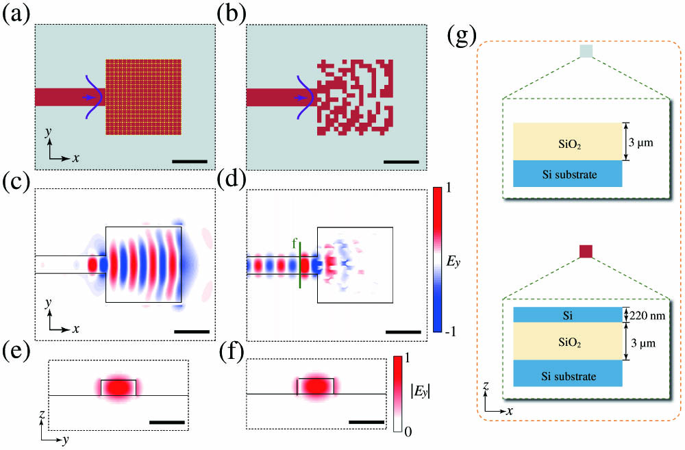
Figure 1.(a) Initial silicon slab before design optimization. (b) Final optimized structure of the on-chip reflector. Field profiles ( component) as the input mode at a wavelength of 1550 nm reflects (c) from the initial silicon slab and (d) from the optimized structure. Field profiles ( component) (e) of the reflected light and (f) of the source at the wavelength of 1550 nm. The scale bars represent 1 μm in (a)–(d) and represent 0.5 μm in (e) and (f). (g) Color code for the vertical structures in (a) and (b). Gray/red pixels denotes the etched/unetched area where no/220-nm silicon layer remains on top of the oxide.
We used a genetic optimization approach to design the on-chip reflector because genetic algorithms are good at global optimization, which can lead to a very high reflectivity in the end. A flow chart of our genetic optimization process [14] is provided in Fig. 2(a). Initializing generation means randomly generating 200 one-dimensional arrays to serve as 200 populations of the first generation. Each array represents the red and gray pixel distribution of a device where “0” in an array represents a gray pixel and “1” represents a red pixel. In the evaluation process, we get the fitness of each population by calculating the reflectivity of the corresponding structure at 1550 nm in Lumerical with three-dimensional finite-difference time-domain simulation. The stop requirement is that the largest fitness either is above 0.99 or does not increase for more than 10 generations. The step of reproducing new generation mainly consists of selection, crossover, and mutation operations. In selection, we used a roulette wheel selection method to select 200 populations from the current generation. Each of the selected 200 populations has 70% probability to have a crossover with another population to produce two new children populations to replace themselves. The detail of the crossover operation is shown in Fig. 2(b), where the crossover point is randomly picked. After crossover, each population in the updated generation has 10% probability of mutation where a random number of pixels are selected to flip. After computation on an 8 core desktop, the fitness did not increase for 10 generations, and we obtained the final optimized structure, as shown in Fig. 1(b).

Figure 2.(a) Flow chart for the genetic optimization process. (b) Illustration showing the crossover process. (c) Reflectivity spectra of the optimized reflector structure (red solid) and of the initial silicon slab (blue dashed). (d) Illustration showing the corner rounding effect. (e) Reflectivity spectra of the optimized reflector considering the corner rounding effect with different rounding radii.
Figures 1(c) and 1(d) show the component of the mode reflected from the initial silicon slab in Fig. 1(a) and from the optimized reflector in Fig. 1(b), respectively, at the wavelength of 1550 nm. Comparing Figs. 1(c) and 1(d), it is clear that the initial silicon slab reflects almost no light but the optimized structure enables total reflection judged from the light intensity on the left of the green line in Fig. 1(d). The green line denotes the light source position in the simulated structure. In addition, the cross-sectional modal profile at a position on the left of the green line in Fig. 1(d) is shown in Fig. 1(e). It is identical to the mode shown in Fig. 1(f), which is the modal profile of the input source. This means that the reflected light faithfully maintains the profile of the mode. Figure 2(c) shows the reflectivity spectra of the optimized reflector (red solid line) and of the initial silicon slab (blue dashed line). The peak reflectivity of the optimized reflector can be as high as 97% and the 1 dB bandwidth is as wide as 220 nm.
During device fabrication, it is usually difficult to make right angles at corners due to the corner rounding effect. Taking this into design consideration, we assumed a nonzero rounding radius at both inner and outer corners, as shown in Fig. 2(d). As the pixel size is in our structure, we set the maximal radius to be 60 nm. Figure 2(e) plots the reflectivity spectra of the optimized reflector with different rounding radii at corners. It is clear that the corner rounding effect plays a negligible role in the device performance.
Highly reflective reflectors are essential parts of high-quality-factor FP cavities. We used the optimized reflectors to construct a FP cavity, as shown in Fig. 3(a). The normalized transmission at the output port can be expressed as [22] where is the coupling coefficient, is the transmission coefficient, is the FP cavity length, and is the mirror reflectivity of the FP cavity. Figure 3(b) plots the normalized transmission spectrum calculated from Eq. (1), where is from the simulation results in Fig. 2(e), is the simulated effective refractive index for a silicon waveguide with a cross section of , is 40 μm, and is fixed at 0.6. Figure 3(c) shows the zoomed-in spectrum of a cavity resonance at .
Figure 3.(a) Layout of an FP cavity constructed from the optimized reflectors. (b) Calculated normalized transmission spectrum of the FP cavity. (c) Normalized transmission spectrum zoomed in at an optical resonance at .
3. EXPERIMENTAL RESULTS AND DISCUSSION
We fabricated the FP cavities on an SOI wafer with a 220 nm Si device layer on 3 μm buried oxide. The patterns of the optimized reflectors were defined along with the connecting waveguides in a single step of electron-beam lithography with ZEP520A resist. The top silicon layer was then etched by using an inductively coupled plasma reactive-ion-etching process. Figure 4(a) is an optical microscope image of an FP cavity device. Figures 4(b) and 4(c) are scanning electron microscope (SEM) images zoomed in at the grating coupler and at the reflector, which has a footprint of only . We fabricated several FP cavity devices with grating couplers of different working spectra to overcome the limitation that the grating couplers usually have their operating bandwidths (often several tens of nanometers) narrower than the optimized reflector. By stitching the individual spectra together, we can get the spectrum in a wide wavelength range.
Figure 4.(a) Optical microscope image of an FP cavity device. (b) Zoomed-in SEM image of the left grating coupler. (c) Zoomed-in SEM image of the right reflector.
The fabricated devices were characterized by spectroscopic measurement of their optical transmission. Light from a tunable semiconductor laser (wavelength range of 1440–1640 nm) was sent over a single-mode fiber into the device via the input grating coupler, with the polarization state controlled by a fiber polarization controller. The transmitted light coupled out of the output grating coupler was collected by a photodetector. Figure 5(a) plots the measured normalized transmission spectrum of the FP cavity device, which is composed of four spectra of devices each with a pair of grating couplers covering a different wavelength band. It is understandable that the spectra may not be perfectly joined at the stitching points due to unavoidable fabrication imperfections. Figures 5(b) and 5(c) show the zoomed-in transmission spectra at and , where the fitted intrinsic quality factors are and , respectively. The similar quality factors of the fabricated and calculated FP cavities have also confirmed the high reflectivity from the fabricated optimized reflectors. The corner rounding effect in fabrication, as clearly seen in the device’s SEM image [Fig. 4(c)], has not affected the reflector’s performance in measurement.
Figure 5.(a) Normalized transmission spectrum of an FP cavity device. The wide-range spectrum is composed of spectra measured from four devices with identical FP cavities but different grating couplers to cover different wavelength bands. The red dashed lines denote the stitching points of the spectra. Zoomed-in spectra showing optical resonances at (b) 1443 and (c) 1620 nm, each fitted with a Lorentzian resonance line shape (red).
Figure 6 shows the reflectivity spectra simulated from the ideal structure (blue solid line), simulated from the fabricated device (black dashed line), and derived from experimental measurement (red dots). The experimental reflectivities were derived from the measured FP cavity quality factors by fitting the cavity resonances using Eq. (1). The simulation for the fabricated structure was conducted by constructing a three-dimensional model in Lumerical based on the device’s SEM image. It is clear that the reflectivity from the experimental measurement maintains higher than 85% in 1440–1640 nm and is even higher than 95% at some cavity resonances. All the simulated and experimental results have proven that the fabricated reflectors possess high reflectivity in a wide spectral range. Looking forward, to further improve the optimization process, we may impose to the structure a mirror symmetry with respect to the plane that cuts through the center axis of the waveguide for optimizing the optical fields of the same symmetry, which should reduce the optimization time.
Figure 6.Reflectivity spectra of the optimized reflectors simulated for the ideal structure (blue solid line), simulated for the fabricated structure (black dashed line), and derived from the experimentally measured FP cavity quality factors (red dots).
4. CONCLUSION
In conclusion, we have proposed a new method for designing on-chip reflectors with high robustness against the corner rounding effect in device fabrication on the thin-film-on-insulator platform. The design relies on a genetic-algorithm optimization method, which can be performed with a normal desktop computer. We also experimentally demonstrated such on-chip reflectors and FP cavities constructed from these reflectors on an SOI wafer. The device fabrication involves only a single step of electron-beam lithography and subsequent dry etching. With a footprint of only , the fabricated reflectors have achieved the expected reflectivity of in the measured wavelength range of 1440–1640 nm, with the best values beyond 95%.
References
[1] T. Mukaihara, N. Yamanaka, N. Iwai, M. Funabashi, S. Arakawa, T. Ishikawa, A. Kasukawa. Integrated GaInAsP laser diodes with monitoring photodiodes through semiconductor/air Bragg reflector (SABAR). IEEE J. Sel. Top. Quantum Electron., 5, 469-475(1999).
[2] S. R. Selmic, G. A. Evans, T. M. Chou, J. B. Kirk, J. N. Walpole, J. P. Donnelly, C. T. Harris, L. J. Missaggia. Single frequency 1550-nm AlGaInAs-InP tapered high-power laser with a distributed Bragg reflector. IEEE Photon. Technol. Lett., 14, 890-892(2002).
[3] B. Docter, T. Segawa, T. Kakitsuka, S. Matsuo, T. Ishii, Y. Kawaguchi, Y. Kondo, H. Suzuki, F. Karouta, M. K. Smit. Short cavity DBR laser using vertical groove gratings for large-scale photonic integrated circuits. IEEE Photon. Technol. Lett., 19, 1469-1471(2007).
[4] C. A. Barrios, V. R. Almeida, R. R. Panepucci, B. S. Schmidt, M. Lipson. Compact silicon tunable Fabry–Perot resonator with low power consumption. IEEE Photon. Technol. Lett., 16, 506-508(2004).
[5] M. W. Pruessner, T. H. Stievater, W. S. Rabinovich. Integrated waveguide Fabry–Perot microcavities with silicon/air Bragg mirrors. Opt. Lett., 32, 533-535(2007).
[6] S. Chen, Y. Shi, S. He, D. Dai. Variable optical attenuator based on a reflective Mach–Zehnder interferometer. Opt. Commun., 361, 55-58(2016).
[7] Y. Wang, S. Gao, K. Wang, H. Li, E. Skafidas. Ultra-broadband, compact, and high-reflectivity circular Bragg grating mirror based on 220 nm silicon-on-insulator platform. Opt. Express, 25, 6653-6663(2017).
[8] N. Ulbrich, G. Scarpa, A. Sigl, J. Roßkopf, G. Böhm, G. Abstreiter, M.-C. Amann. High-temperature (T ≥ 470 K) pulsed operation of 5.5 μm quantum cascade lasers with high-reflection coating. Electron. Lett., 37, 1341-1342(2001).
[9] S. Zamek, L. Feng, M. Khajavikhan, D. T. H. Tan, M. Ayache, Y. Fainman. Micro-resonator with metallic mirrors coupled to a bus waveguide. Opt. Express, 19, 2417-2425(2011).
[10] J. Canning, N. Skivesen, M. Kristensen, L. H. Frandsen, A. Lavrinenko, C. Martelli, A. Tetu. Mapping the broadband polarization properties of linear 2D SOI photonic crystal waveguides. Opt. Express, 15, 15603-15614(2007).
[11] L. H. Frandsen, Y. Elesin, O. Sigmund, K. Yvind. Topology optimization of coupled photonic crystal cavities for flat-top drop filter functionality. European Conference on Lasers and Electro-Optics-European Quantum Electronics Conference, CK_9_1(2015).
[12] L. H. Frandsen, Y. Elesin, L. F. Frellsen, M. Mitrovic, Y. Ding, O. Sigmund, K. Yvind. Topology optimized mode conversion in a photonic crystal waveguide fabricated in silicon-on-insulator material. Opt. Express, 22, 8525-8532(2014).
[13] J. S. Jensen, O. Sigmund. Topology optimization for nano-photonics. Laser Photon. Rev., 5, 308-321(2011).
[14] Z. Yu, H. Cui, X. Sun. Genetic-algorithm-optimized wideband on-chip polarization rotator with an ultrasmall footprint. Opt. Lett., 42, 3093-3096(2017).
[15] A. Y. Piggott, J. Lu, K. G. Lagoudakis, J. Petykiewicz, T. M. Babinec, J. Vučković. Inverse design and demonstration of a compact and broadband on-chip wavelength demultiplexer. Nat. Photonics, 9, 374-377(2015).
[16] B. Shen, P. Wang, R. Polson, R. Menon. An integrated-nanophotonics polarization beamsplitter with 2.4 × 2.4 μm2 footprint. Nat. Photonics, 9, 378-382(2015).
[17] J. C. C. Mak, C. Sideris, J. Jeong, A. Hajimiri, J. K. S. Poon. Binary particle swarm optimized 2 × 2 power splitters in a standard foundry silicon photonic platform. Opt. Lett., 41, 3868-3871(2016).
[18] K. Xu, L. Liu, X. Wen, W. Sun, N. Zhang, N. Yi, S. Sun, S. Xiao, Q. Song. Integrated photonic power divider with arbitrary power ratios. Opt. Lett., 42, 855-858(2017).
[19] L. F. Frellsen, Y. Ding, O. Sigmund, L. H. Frandsen. Topology optimized mode multiplexing in silicon-on-insulator photonic wire waveguides. Opt. Express, 24, 16866-16873(2016).
[20] Y. A. Vlasov, S. J. McNab. Losses in single-mode silicon-on-insulator strip waveguides and bends. Opt. Express, 12, 1622-1631(2004).
[21] J. Wu, T. Moein, X. Xu, G. Ren, A. Mitchell, D. J. Moss. Micro-ring resonator quality factor enhancement via an integrated Fabry–Perot cavity. APL Photon., 2, 056103(2017).
[22] D. G. Rabus. Integrated Ring Resonators(2007).


