Hong-Jie GUO, Hai-Feng LIU, Zhen-Nuo WANG, Man-Qing TAN, Zhi-Yong LI, Ming Lei, Wen-Tao GUO. Design of a novel Y-junction electro-optic modulator based on thin film lithium niobite[J]. Journal of Infrared and Millimeter Waves, 2022, 41(3): 626
Copy Citation Text
In recent years, the high-performance electro-optic modulator based on the thin-film lithium niobate (TFLN) platform has been receiving considerable attention due to the featuring small footprint and low energy loss. In this paper, a novel Y-junction electro-optic modulator with a vertical electrode structure was designed based on TFLN. The relationship between the low half-wave voltage and the buffer layer thickness for the novel modulator was investigated. Meanwhile, the design parameters of Y-junction were optimized, and found that the half-wave voltage is less than 1.5 V and the insertion loss is less than 5 dB. Finally, the Y-junction electro-optic modulator was fabricated. This study not only provides insights on the design and realization of compact footprint photonic waveguides in the TFLN platform but also, experimental evidence for the fabrication of electro-optic modulators with high-performance and multifunction.
In the last decades,photonic integrated circuits(PICs)have emerged as a mature and industrial platform,enabling the integration of active and passive optical components on a single chip in a scalable manner. Prominent PIC platforms,which are being developed to industrial scale,are silicon on insulator(SOI)[1,2],silicon nitride(SiN)[3,4],indium phosphate(InP)[5,6],and lithium niobate(LN)[7,8]. Lithium niobate(LiNbO3,LN)is one of the most remarkable optical platforms due to its broad transparent windows and excellent electro-optic properties(γ33= 31.2 pm/V). LN phase modulator(PM)is utilized as a tool to convert electrical signals into optical signals,and that plays vital roles in optical communication networks[9,10],precision optical sensors[11,12],quantum photonics[13],and non-reciprocal optics[14,15].
Size and power efficiency are crucial to the application of the LN modulator. Conventional LN modulators are formed by low-index-contrast waveguides with weak optical confinement,which leads to the radius of bending and other adiabatic waveguides even up to 30 mm[16]. And the electrodes must be placed far away from the optical waveguide to minimize absorption losses,which leads to an increased drive voltage[17]. As a result,the conventional LN modulators are bulky in size and low in modulation efficiency(Vπ L> 10 V cm)[18,19]. Recently,thin-film lithium niobate(TFLN)has emerged as a promising platform for excellent and compact electro-optic modulator,which unlocks new levels of performance and footprint in LN modulators because it overcomes the fundamental voltage-size trade-off in conventional low-index-contrast LN modulators[20,21].
In this paper,a novel Y-junction electro-optic PM based on the TFLN platform was analyzed,simulated,and designed. The low half-wave voltage versus the thickness of the buffer layer was analyzed. The propagation losses of LN waveguides with different separation distances were optimized using the Beam Propagation Method(BPM). Finally,the designed electro-optic modulator features low optical loss(<5 dB),low (<1.5 V),and a small footprint(<2 cm),compared with the conventional LN counterpart. The results obtained in this paper can provide useful insight into the design of high-performance and multifunction electro-optic modulators.
1 Design and materials
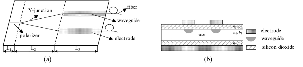
The device studied in this paper was a Z-cut TFLN deposited on an LN substrate,which utilizes the maximum electro-optic coefficient γ33. Fig. 1(a)shows the schematic diagram of the TFLN electro-optic PM. In Fig. 1(a),The polarizer(L1)is realized with a metallic overlay that absorbs the TM mode,which could provide high polarization rejection based on a proton exchange waveguide. The Y-junction(L2)is a 3 dB passive waveguide coupler,which is the optimal technological compromise for high-performance fiber optical gyroscopes(FOG). Metallic electrodes are fabricated vertically above the waveguide to achieve phase modulation(L3). The end-face coupling technique is employed to couple the LN substrate with the fiber. Fig. 1(b)shows the cross-section of the TFLN modulator. The vertical electrode configuration based on the TFLN slab not only reduces the electrode gap but also increases the integral Γ as shown in Fig. 1(b). To avoid optical absorption resulting from the electrodes placed directly above the waveguide,a buffer layer of SiO2 thin film was inserted between the TFLN slab and the electrodes.
Figure 1.(a)The schematic diagram of the TFLN PM,(b)the cross section of the TFLN PM
When the light wave travels through a modulation length of L,the phase change can be expressed as:
,
where Δβ is the change of propagation constant induced by the applied electric field,ne is the refractive index of the extraordinary lightwave,Δneis the change of refractive index induced by the applied electric field,γ33 is the electro-optic coefficient of lithium niobite crystal,E is applied electric field in the waveguide,and Γ is the electro-optic integral factor between the electric field and optical field.
For the traditional bulk LN PM,the applied voltage corresponding to a phase change of π,generally known as half-wave voltage,can be expressed as:
.
According to Eq.(2),it is found that the proper method of decreasing Vπ for a fixed modulation length L is to narrow the electrode gap G or improve the electro-optic integral factor Γ. Generally,the electrode gap should be maintained at a certain distance so as to avoid possible optical absorption of the waveguide. The integral Γ cannot be increased dramatically for the coplanar electrode structure on the surface of the LN crystal. Therefore,the above methods are inappropriate for the traditional LN fabricated on bulk LN PM. The TFLN PM with a vertical electrode is beneficial for shortening the G and increasing the integral Γ simultaneously. Compared to the integral Γ of 40%~50% for the electrode configuration in bulk LN crystal,Γ can be as high as 90~100% for the vertical electrode structure. In Fig. 1(b),the buffer layer thickness is b2 and the corresponding refractive index(n2)is 1.45. The thickness of TFLN slab is b1 and the refractive index(n1)is 2.21. According to the boundary conditions of the electromagnetic fields(see Eq.(3) and Eq.(4)),the Vπof TFLN PM can be expressed as:
,
,
.
Fig. 2(a)shows the Vπ of conditional bulk PM as a function of G at the modulation length L of 5 mm,10 mm,20 mm,and the integral Γ of 50%. Fig. 2(b)shows the Vπ of TFLN PM as a function of b2,with Γ=90% and b1=5 μm. Compared with bulk LN PM,the Vπ of TFLN PM can be dramatically decreased when the same modulation length is adopted. This is beneficial for the high-performance PIC. Moreover,it is also observed that when L>10 mm,the Vπ would be less than 1.5 V. So,to meet the circuit design,the L3=1000 μm is taken into account in our proposed modulator.
Figure 2.(a)The Vπ of conditional bulk PM various G at different modulation length,where Γ = 0.5,(b)the Vπ of TFLN PM various b2 at different modulation length, where Γ = 0.9,b1=5 μm
Fig. 3(a)shows the schematic diagram of the Y-junction composed of two identical S-waveguides. The distance between the S-waveguide,width,height,length,and bending angle of the S-waveguide are denoted as W,w,h,L2,and α,respectively. Fig. 3(b)shows the W as a function of L2 under the different bending angle α. From Fig. 3(b),it is found the W increases with the increase of the modulation length L2. Besides,the W decreases as the bending angle α decreases. In order to cut down the footprint of the modulator and reduce the propagation loss of light,it is also necessary to optimize the parameters of Y-junction waveguide. In addition,W should satisfy the empirical value 150 μm≤W≤400 μm,which matches the V-groove coupling process[22]. So,the light-guiding properties of the Y-junction waveguide(h=7 μm,w=7 μm,Δn=0.015,α=0.4~1.0° and L2=0.4~1.2 cm)are simulated using the BPM method with RSoft commercial software.
Figure 3.(a)The sketch of Y-junction waveguide,(b)the W of Y-junction waveguide versus L2 at different α
Fig. 4(a)shows the normalized input power to the output ports as the input field propagates through the Y-junction. From Fig. 4(a)it can be seen that the output power decreases with the increase of the L2. Besides,the output power also decreases as the bending angle α increases. In order to balance the loss and the manufacturing process,α=0.6° and L2=9000 μm are selected as the optimal parameters. The simulation results of α=0.6° and L2=9000 μm are shown in Fig. 4(b-c). The simulated result(Fig. 4(b))shows the refractive index profile of waveguide section when L2=100 μm. Fig. 4(c)shows the electric field distribution inside the Y-junction waveguide. It is obvious that there exists and clearly shows an almost equal splitting of input power into two branches.
Figure 4.(a)The results of BPM simulation,(b)the refractive index profile of waveguide section,(c)the power distribution of Y-junction waveguide
The overall insertion loss(coupling loss and propagation loss)of the TFLN PM with the 7 μm diameter fiber is simulated using the BPM method by RSoft. The simulation result is shown in Fig. 5. It is can be seen that the overall insertion loss is 4.7 dB. Meanwhile,it is also observed that the coupling loss almost accounts for 94% of the insertion loss,which is caused by the mismatch of the optical mode field. The mode field mismatch loss can be expressed by the following formula Eq.(6)
,
where ϕf(x,y) is the mode field distribution of fiber,ϕw(x,y) is the mode field distribution of waveguide. This paper simulates the result of a direct connection between the flat-end optical fiber and the untreated waveguide end face. Due to the weak ability of the diffused waveguide to restrict the optical field,the diameter of waveguidemode field distribution ϕw(x,y)(about 10 μm)is larger than that of fiber field distribution ϕf(x,y)(6 μm),which leads to a mode field mismatch. The ϕw(x,y) can be reduced by adding a spot-size converter(SSC)to the output of the waveguide,and then a lower coupling loss is obtained.
Fig. 6 shows the cross-section of the TFLN slab bonded on the LN substrate. The anneal proton exchange waveguide(w=7 μm,h=7 μm,L1=1 000 μm, L2=9 000 μm,L3=10 000 μm)was fabricated on the Z-cut thin-film lithium niobite slab on a bulk LN substrate. The bright stripe in the middle is the TFLN slab and the slightly darker area underneath is the bulk LN substrate.
Figure 6.The microscope image of the cross-section of the TFLN slab bonded on the LN substrate
The Z-cut thin-film lithium niobite wafer on bulk LN substrate was fabricated by the direct bonding technology and chemical mechanical polishing process,and a thin film of 10 μm was obtained. Subsequently,the proton exchange process was performed by immersing the TFLN wafer into the benzoic acid melt with lithium benzoate,which started at a temperature of around 200 ℃ and lasted for about 4~5 hours. And afterward,the TFLN chip was placed at the center of a three-zone diffusion furnace. The thermal annealing process was performed at a temperature of around 330 ℃. The wafer was placed at the furnace lasting for several hours. Finally,the TFLN waveguide wafer was diced into individual chips and the endfaces were polished.
The insertion loss of the TFLN waveguide was characterized based on the butt-coupling method at the wavelength of 1310 nm. A polarization-maintaining fiber with a mode field diameter(MFD)of 6.0±0.5 μm was placed at the input port and output port of the TFLN waveguide sample. An insertion loss of ~5.0 dB was obtained using an SLD light source,and it is limited by the waveguide coupling method of the V-groove process. This value could be further increased by the edge coupling method[23].
4 Conclusion
In conclusion,a novel Y-junction electro-optic PM was analyzed,simulated,and designed. The correlation of the low half-wave voltage and thickness of the buffer layer was analyzed. It is found there exists a negative correlation between the low half-wave voltage and thickness of the buffer layer. The Vπ of TFLN PM can be dramatically decreased when the same modulation length is adopted compared with that of the bulk LN PM,which is beneficial for the high-performance PIC. Moreover,the propagation losses of LN waveguides with different separation distances of the waveguide were optimized by the BPM method. It is found that the overall insertion loss is 4.7 dB. Finally,an on-chip PM with low optical loss(<5 dB)and a smaller footprint(<2 cm)was fabricated.
[15] W Xue, Z Qiao-Fen, Z Yan. Generation of arbitrary terahertz pulse in non periodically poled lithium niobate. J.Infrared Millim.Waves, 30, 221-223(2010).
[22] T Zijun, C Wenfeng, W Hao et al. Research on Direct Couping of PM Fiber Coil and Y-branch LiNbO3 Waveguide Chip. Semiconductor Optoelectronics, 38, 57-60(2017).
Hong-Jie GUO, Hai-Feng LIU, Zhen-Nuo WANG, Man-Qing TAN, Zhi-Yong LI, Ming Lei, Wen-Tao GUO. Design of a novel Y-junction electro-optic modulator based on thin film lithium niobite[J]. Journal of Infrared and Millimeter Waves, 2022, 41(3): 626