• Journal of Infrared and Millimeter Waves
  • Vol. 41, Issue 3, 626 (2022)
Hong-Jie GUO1、3, Hai-Feng LIU1、*, Zhen-Nuo WANG2、3, Man-Qing TAN1、3、**, Zhi-Yong LI1, Ming Lei3, and Wen-Tao GUO1
Author Affiliations
  • 1State Key Laboratory of Integrated Optoelectronics,Institute of Semiconductors,Chinese Academy of Sciences,Beijing 100083,China
  • 2National Engineering Research Center for Optoelectronic Devices,Institute of Semiconductors,Chinese Academy of Sciences,Beijing 100083,China
  • 3College of Materials Science and Opto-electronics Technology,University of Chinese Academy of Sciences,Beijing 100049,China
  • show less
    DOI: 10.11972/j.issn.1001-9014.2022.03.014 Cite this Article
    Hong-Jie GUO, Hai-Feng LIU, Zhen-Nuo WANG, Man-Qing TAN, Zhi-Yong LI, Ming Lei, Wen-Tao GUO. Design of a novel Y-junction electro-optic modulator based on thin film lithium niobite[J]. Journal of Infrared and Millimeter Waves, 2022, 41(3): 626 Copy Citation Text show less
    (a)The schematic diagram of the TFLN PM,(b)the cross section of the TFLN PM
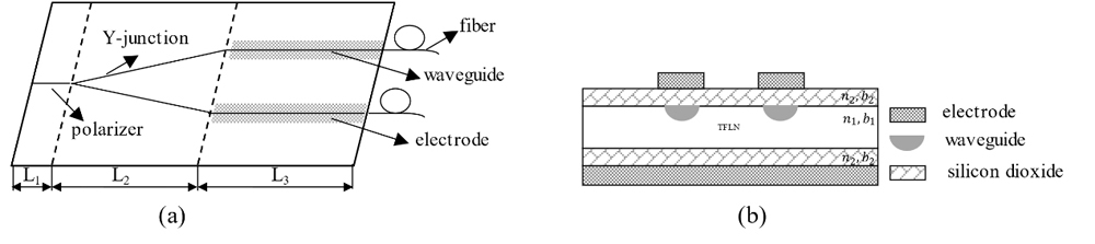
    Fig. 1. (a)The schematic diagram of the TFLN PM,(b)the cross section of the TFLN PM
    (a)The Vπ of conditional bulk PM various G at different modulation length,where Γ = 0.5,(b)the Vπ of TFLN PM various b2 at different modulation length, where Γ = 0.9,b1=5 μm
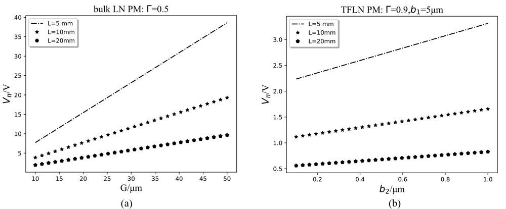
    Fig. 2. (a)The Vπ of conditional bulk PM various G at different modulation length,where Γ = 0.5,(b)the Vπ of TFLN PM various b2 at different modulation length where Γ = 0.9,b1=5 μm
    (a)The sketch of Y-junction waveguide,(b)the W of Y-junction waveguide versus L2 at different α
    Fig. 3. (a)The sketch of Y-junction waveguide,(b)the W of Y-junction waveguide versus L2 at different α
    (a)The results of BPM simulation,(b)the refractive index profile of waveguide section,(c)the power distribution of Y-junction waveguide
    Fig. 4. (a)The results of BPM simulation,(b)the refractive index profile of waveguide section,(c)the power distribution of Y-junction waveguide
    The results of simulation modulator insertion loss,where L1=1 000 μm,L2=9 000 μm,L3=10 000 μm,α=0.6°
    Fig. 5. The results of simulation modulator insertion loss,where L1=1 000 μm,L2=9 000 μm,L3=10 000 μm,α=0.6°
    The microscope image of the cross-section of the TFLN slab bonded on the LN substrate
    Fig. 6. The microscope image of the cross-section of the TFLN slab bonded on the LN substrate
    Hong-Jie GUO, Hai-Feng LIU, Zhen-Nuo WANG, Man-Qing TAN, Zhi-Yong LI, Ming Lei, Wen-Tao GUO. Design of a novel Y-junction electro-optic modulator based on thin film lithium niobite[J]. Journal of Infrared and Millimeter Waves, 2022, 41(3): 626
    Download Citation