• Photonics Insights
  • Vol. 2, Issue 2, R04 (2023)
Hyunjung Kang1、†, Dohyeon Lee1, Younghwan Yang1, Dong Kyo Oh1, Junhwa Seong1, Jaekyung Kim1, Nara Jeon1, Dohyun Kang1, and Junsuk Rho1、2、3、*
Author Affiliations
  • 1Department of Mechanical Engineering, Pohang University of Science and Technology (POSTECH), Pohang, Republic of Korea
  • 2Department of Chemical Engineering, Pohang University of Science and Technology (POSTECH), Pohang, Republic of Korea
  • 3POSCO-POSTECH-RIST Convergence Research Center for Flat Optics and Metaphotonics, Pohang, Republic of Korea
  • show less
    DOI: 10.3788/PI.2023.R04 Cite this Article Set citation alerts
    Hyunjung Kang, Dohyeon Lee, Younghwan Yang, Dong Kyo Oh, Junhwa Seong, Jaekyung Kim, Nara Jeon, Dohyun Kang, Junsuk Rho. Emerging low-cost, large-scale photonic platforms with soft lithography and self-assembly[J]. Photonics Insights, 2023, 2(2): R04 Copy Citation Text show less
    Large-area, low-cost fabrication methods are introduced as follows: nanoimprint lithography, transfer printing, capillary force lithography, block copolymer self-assembly, and colloidal photonic crystal self-assembly.
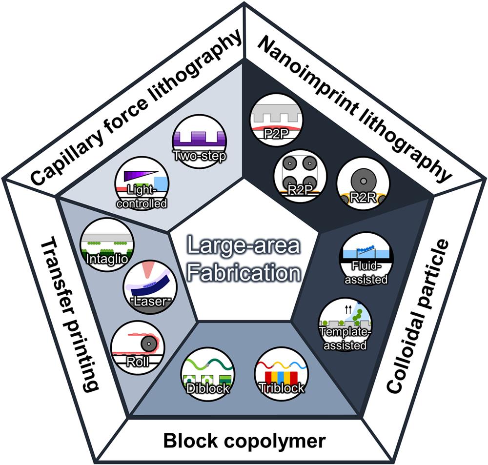
    Fig. 1. Large-area, low-cost fabrication methods are introduced as follows: nanoimprint lithography, transfer printing, capillary force lithography, block copolymer self-assembly, and colloidal photonic crystal self-assembly.
    Types of nanoimprint lithography (NIL) depending on curing stimuli and contact types. (a) NIL variants based on resist curing. (i) NIL processes using a photopolymer resist, whose curing trigger is UV light. (ii) NIL processes using a thermoplastic polymer resist, whose curing trigger is heat. (b) NIL variants based on imprint contact types. (i) P2P NIL processes through contact between flat stamp and substrate. Reprinted with permission from Ref. [41], copyright 2021, American Chemical Society. (ii) R2R NIL processes using a pattern roller. Reprinted with permission from Ref. [45], copyright 2015, American Vacuum Society. (iii) R2P NIL processes through contact between rollers and flat substrate. Reprinted with permission from Ref. [47], copyright 2022, Multidisciplinary Digital Publishing Institute.
    Fig. 2. Types of nanoimprint lithography (NIL) depending on curing stimuli and contact types. (a) NIL variants based on resist curing. (i) NIL processes using a photopolymer resist, whose curing trigger is UV light. (ii) NIL processes using a thermoplastic polymer resist, whose curing trigger is heat. (b) NIL variants based on imprint contact types. (i) P2P NIL processes through contact between flat stamp and substrate. Reprinted with permission from Ref. [41], copyright 2021, American Chemical Society. (ii) R2R NIL processes using a pattern roller. Reprinted with permission from Ref. [45], copyright 2015, American Vacuum Society. (iii) R2P NIL processes through contact between rollers and flat substrate. Reprinted with permission from Ref. [47], copyright 2022, Multidisciplinary Digital Publishing Institute.
    Various applications using the NIL. (a) (i) Thermal R2R NIL for an antireflective film. The processes go on under a certain range of pressure (P) and temperature (T). (ii) Measured total reflection spectrum. (iii) Scanning electron microscope (SEM) image of imprinted moth-eye structures at 140°C. Inset: 3D reconstructions of atomic force microscope (AFM) images of imprinted areas. Reprinted with permission from Ref. [58], copyright 2021, Springer Nature. (b) (i) P2P NIL for an infrared nanowire grid polarizer. (ii) TM and TE transmittance spectrum. (iii) Photograph of the polarizer with 4-inch area. Reprinted with permission from Ref. [59], copyright 2018, Optica. (c) (i) Schematic of the P2P NIL for solar cells with grating structures. (ii) Power–voltage graph of solar cells with/without grating structures. (iii) Side view of the SEM image of grating structures via imprinting with vibration. Reprinted with permission from Ref. [60], copyright 2022, Elsevier. (d) (i) P2P NIL using particle-embedded resist (PER) for metasurfaces. (ii) Calculated hologram efficiency. (iii) Simulated/generated holographic images of metasurfaces. Reprinted with permission from Ref. [61], copyright 2019, American Chemical Society.
    Fig. 3. Various applications using the NIL. (a) (i) Thermal R2R NIL for an antireflective film. The processes go on under a certain range of pressure (P) and temperature (T). (ii) Measured total reflection spectrum. (iii) Scanning electron microscope (SEM) image of imprinted moth-eye structures at 140°C. Inset: 3D reconstructions of atomic force microscope (AFM) images of imprinted areas. Reprinted with permission from Ref. [58], copyright 2021, Springer Nature. (b) (i) P2P NIL for an infrared nanowire grid polarizer. (ii) TM and TE transmittance spectrum. (iii) Photograph of the polarizer with 4-inch area. Reprinted with permission from Ref. [59], copyright 2018, Optica. (c) (i) Schematic of the P2P NIL for solar cells with grating structures. (ii) Power–voltage graph of solar cells with/without grating structures. (iii) Side view of the SEM image of grating structures via imprinting with vibration. Reprinted with permission from Ref. [60], copyright 2022, Elsevier. (d) (i) P2P NIL using particle-embedded resist (PER) for metasurfaces. (ii) Calculated hologram efficiency. (iii) Simulated/generated holographic images of metasurfaces. Reprinted with permission from Ref. [61], copyright 2019, American Chemical Society.
    Mechanisms of different transfer printing methods. (a) Transfer printing processes using an intaglio trench, which allows only the desired pattern to remain on the stamp without any morphological changes. Reprinted with permission from Ref. [80], copyright 2022, American Chemical Society. (b) Laser-driven transfer printing processes. Selectively heating the inks via laser induces strong thrust between stamp and inks, forming a pattern on receiver. Reprinted with permission from Ref. [83], copyright 2021, John Wiley and Sons. (c) Direct roll transfer printing processes. Si nanoribbons (NRs) are released by undercut etching of the buried oxide (box) (scale bar 10 µm, red line), and then brought into direct contact with semi-cured polyimide (PI) thin film (scale bar 25 µm, black line). Reprinted with permission from Ref. [85], copyright 2021, Springer Nature.
    Fig. 4. Mechanisms of different transfer printing methods. (a) Transfer printing processes using an intaglio trench, which allows only the desired pattern to remain on the stamp without any morphological changes. Reprinted with permission from Ref. [80], copyright 2022, American Chemical Society. (b) Laser-driven transfer printing processes. Selectively heating the inks via laser induces strong thrust between stamp and inks, forming a pattern on receiver. Reprinted with permission from Ref. [83], copyright 2021, John Wiley and Sons. (c) Direct roll transfer printing processes. Si nanoribbons (NRs) are released by undercut etching of the buried oxide (box) (scale bar 10 µm, red line), and then brought into direct contact with semi-cured polyimide (PI) thin film (scale bar 25 µm, black line). Reprinted with permission from Ref. [85], copyright 2021, Springer Nature.
    Various applications of transfer printing. (a) (i) Transfer printing integrated with post-assembly to fabricate the sub-10 nm nanogap. A gold nanodimer with 120 nm gap size is transferred onto pre-stretched polydimethylsiloxane (PDMS) substrate, which then is released. After releasing the substrate, the large gap in dimer is shrunk (∼5 nm). (ii) Photoluminescence (PL) spectra of MoS2 flake with the post-assembled nanodimer (red line) and initial nanodimer (orange line). (iii) SEM images of gold nanodimer before and after releasing the stress. Reprinted with permission from Ref. [101], copyright 2020, John Wiley and Sons. (b) (i) Synthesizing and transfer printing processes of ZnO nanostructures on a polycarbonate (PC) substrate. (ii) Transmittance spectra of A series and B series. A series represents as-grown nanorod arrays, and the corresponding transferred nanorod arrays with 60 s O2 treatment are represented as B series. Inset: SEM images of transferred nanorod arrays. Reprinted with permission from Ref. [109], copyright 2022, John Wiley and Sons.
    Fig. 5. Various applications of transfer printing. (a) (i) Transfer printing integrated with post-assembly to fabricate the sub-10 nm nanogap. A gold nanodimer with 120 nm gap size is transferred onto pre-stretched polydimethylsiloxane (PDMS) substrate, which then is released. After releasing the substrate, the large gap in dimer is shrunk (5nm). (ii) Photoluminescence (PL) spectra of MoS2 flake with the post-assembled nanodimer (red line) and initial nanodimer (orange line). (iii) SEM images of gold nanodimer before and after releasing the stress. Reprinted with permission from Ref. [101], copyright 2020, John Wiley and Sons. (b) (i) Synthesizing and transfer printing processes of ZnO nanostructures on a polycarbonate (PC) substrate. (ii) Transmittance spectra of A series and B series. A series represents as-grown nanorod arrays, and the corresponding transferred nanorod arrays with 60 s O2 treatment are represented as B series. Inset: SEM images of transferred nanorod arrays. Reprinted with permission from Ref. [109], copyright 2022, John Wiley and Sons.
    Developments in capillary force lithography (CFL) methods. (a) Optically height-controlled CFL processes. A UV-curable polymer, NOA73, is precured by UV irradiation with different UV doses for each of the four division areas. This leads to thickness difference of the liquid-phase photopolymer layer (scale bar 1 µm). Reprinted with permission from Ref. [114], copyright 2020, American Chemical Society. (b) Continuous fabrication processes via two-step CFL. Polyurethane acrylate (PUA) resin is partially cured by UV irradiation, and top portion of the resin is completely cured with pressure.
    Fig. 6. Developments in capillary force lithography (CFL) methods. (a) Optically height-controlled CFL processes. A UV-curable polymer, NOA73, is precured by UV irradiation with different UV doses for each of the four division areas. This leads to thickness difference of the liquid-phase photopolymer layer (scale bar 1 µm). Reprinted with permission from Ref. [114], copyright 2020, American Chemical Society. (b) Continuous fabrication processes via two-step CFL. Polyurethane acrylate (PUA) resin is partially cured by UV irradiation, and top portion of the resin is completely cured with pressure.
    Various applications of CFL. (a) (i) Perovskite patterning method using CFL. (ii) External quantum efficiency (EQE) spectra of micro-PeLEDs with 0.06%, 0.08%, 0.10%, and 0.12% (mass fractions) poly(ethylene oxide) (PEO). (iii) Light-emitting images of the micro-PeLEDs with 0.06% and 0.10% PEO. Reprinted with permission from Ref. [129], copyright 2022, Elsevier. (b) (i) Ag nanowire (AgNW) solution patterning using CFL. Hydrogel infiltrated at the edge of the PDMS stamp is cured on the patterned AgNWs by UV irradiation, and then washed off by ethanol. After ethanol washing, hydrogel-free AgNWs remain. (ii) Gauge factor as a function of applied tensile strain. (iii) Field emission SEM image of the patterned AgNWs on glass. Reprinted with permission from Ref. [131], copyright 2017, American Chemical Society.
    Fig. 7. Various applications of CFL. (a) (i) Perovskite patterning method using CFL. (ii) External quantum efficiency (EQE) spectra of micro-PeLEDs with 0.06%, 0.08%, 0.10%, and 0.12% (mass fractions) poly(ethylene oxide) (PEO). (iii) Light-emitting images of the micro-PeLEDs with 0.06% and 0.10% PEO. Reprinted with permission from Ref. [129], copyright 2022, Elsevier. (b) (i) Ag nanowire (AgNW) solution patterning using CFL. Hydrogel infiltrated at the edge of the PDMS stamp is cured on the patterned AgNWs by UV irradiation, and then washed off by ethanol. After ethanol washing, hydrogel-free AgNWs remain. (ii) Gauge factor as a function of applied tensile strain. (iii) Field emission SEM image of the patterned AgNWs on glass. Reprinted with permission from Ref. [131], copyright 2017, American Chemical Society.
    Types of colloidal self-assembly techniques. (a) Fluid-assisted convective self-assembly. As the solvent evaporation induces a convective flow, the colloidal particles form arrays owing to the capillary force acting between them. (b) Colloidal self-assembly by using Langmuir–Blodgett method. By compressing the barrier, the monolayer is produced and then deposited on the vertically/horizontally positioned substrate. (c) Colloidal self-assembly by using Marangoni effect. Exposing a nanoparticle (NP)/ethanol (EH) suspension to a wet nitrogen (N2) stream induces the evaporation of EH and the condensation of water (H2O). This leads to the surface tension gradient [EH (γ=22 mN/m) and H2O (γ=72 mN/m)], driving the NPs/H2O toward the receding contact line. (d) Template-assisted self-assembly for plasmonic nanoarray. Photoresist is spread onto the antireflection coated (ARC) Si, and then imprinted to form a PDMS template. The template is used to align the colloidal plasmonic nanoparticles in a 2D square lattice. Right: SEM images of the fabricated master mold, PDMS nanohole arrays, and 2D plasmonic lattice. Reprinted with permission from Ref. [182], copyright 2019, American Chemistry Society.
    Fig. 8. Types of colloidal self-assembly techniques. (a) Fluid-assisted convective self-assembly. As the solvent evaporation induces a convective flow, the colloidal particles form arrays owing to the capillary force acting between them. (b) Colloidal self-assembly by using Langmuir–Blodgett method. By compressing the barrier, the monolayer is produced and then deposited on the vertically/horizontally positioned substrate. (c) Colloidal self-assembly by using Marangoni effect. Exposing a nanoparticle (NP)/ethanol (EH) suspension to a wet nitrogen (N2) stream induces the evaporation of EH and the condensation of water (H2O). This leads to the surface tension gradient [EH(γ=22mN/m) and H2O (γ=72mN/m)], driving the NPs/H2O toward the receding contact line. (d) Template-assisted self-assembly for plasmonic nanoarray. Photoresist is spread onto the antireflection coated (ARC) Si, and then imprinted to form a PDMS template. The template is used to align the colloidal plasmonic nanoparticles in a 2D square lattice. Right: SEM images of the fabricated master mold, PDMS nanohole arrays, and 2D plasmonic lattice. Reprinted with permission from Ref. [182], copyright 2019, American Chemistry Society.
    Various applications of colloidal self-assembly structures. (a) (i) In situ chemical patterning processes for surface-enhanced Raman scattering (SERS) substrate. (ii) Raman spectra under different LED illumination times (30, 60, 90, and 120 min). Right: SEM images of the Ag nanoparticle array (scale bar 100 nm). Reprinted with permission from Ref. [213], copyright 2022, John Wiley and Sons. (b) (i) Multiple-patterning for a ring-shaped absorber. Right: SEM images after second polystyrene (PS) size reduction and PS removal. (ii) Absorption contributions of each TiN layer. Total power dissipation density of top ring-shaped TiN nanostructure (red line), bottom TiN layer (blue line), and the summation of two densities (black line). Reprinted with permission from Ref. [221], copyright 2021, Springer Nature. (c) (i) Colloidal self-assembly processes for anisotropic Janus structural color particles (SCPs) by phase separation and cardiomyocyte monitoring platform. (ii) Reflective peaks and reflection images of five different anisotropic Janus SCPs. (iii) SEM images of whole (black line, scale bar 100 µm), colorful hemispherical section (yellow line, scale bar 1 µm), and black oblate section (red line, scale bar 2 µm) of anisotropic Janus SCPs. Reprinted with permission from Ref. [225], copyright 2020, American Association for the Advancement of Science.
    Fig. 9. Various applications of colloidal self-assembly structures. (a) (i) In situ chemical patterning processes for surface-enhanced Raman scattering (SERS) substrate. (ii) Raman spectra under different LED illumination times (30, 60, 90, and 120 min). Right: SEM images of the Ag nanoparticle array (scale bar 100 nm). Reprinted with permission from Ref. [213], copyright 2022, John Wiley and Sons. (b) (i) Multiple-patterning for a ring-shaped absorber. Right: SEM images after second polystyrene (PS) size reduction and PS removal. (ii) Absorption contributions of each TiN layer. Total power dissipation density of top ring-shaped TiN nanostructure (red line), bottom TiN layer (blue line), and the summation of two densities (black line). Reprinted with permission from Ref. [221], copyright 2021, Springer Nature. (c) (i) Colloidal self-assembly processes for anisotropic Janus structural color particles (SCPs) by phase separation and cardiomyocyte monitoring platform. (ii) Reflective peaks and reflection images of five different anisotropic Janus SCPs. (iii) SEM images of whole (black line, scale bar 100 µm), colorful hemispherical section (yellow line, scale bar 1 µm), and black oblate section (red line, scale bar 2 µm) of anisotropic Janus SCPs. Reprinted with permission from Ref. [225], copyright 2020, American Association for the Advancement of Science.
    Morphology of block copolymer (BCP) self-assembly structure. (a) Different phases formed by diblock copolymer self-assembly depending on fA (fA, volume fraction of block A). Reprinted with permission from Ref. [228], copyright 2006, American Chemical Society. (b) (i) Morphology of ABC triblock copolymer. (ii) Structure of ABA triblock copolymer based on B-selective solvent. Reprinted with permission from Ref. [230], copyright 2015, Elsevier. (c) Orthogonal self-assembly processes for multilayer structure. Reprinted with permission from Ref. [232], copyright 2016, Springer Nature. (d) Self-directed self-assembly processes of aligned multilayer structure. Right: cross section of the multilayer structure after self-assembly in the dissipative particle dynamics (DPD) simulation. Reprinted with permission from Ref. [233], copyright 2020, American Chemical Society.
    Fig. 10. Morphology of block copolymer (BCP) self-assembly structure. (a) Different phases formed by diblock copolymer self-assembly depending on fA (fA, volume fraction of block A). Reprinted with permission from Ref. [228], copyright 2006, American Chemical Society. (b) (i) Morphology of ABC triblock copolymer. (ii) Structure of ABA triblock copolymer based on B-selective solvent. Reprinted with permission from Ref. [230], copyright 2015, Elsevier. (c) Orthogonal self-assembly processes for multilayer structure. Reprinted with permission from Ref. [232], copyright 2016, Springer Nature. (d) Self-directed self-assembly processes of aligned multilayer structure. Right: cross section of the multilayer structure after self-assembly in the dissipative particle dynamics (DPD) simulation. Reprinted with permission from Ref. [233], copyright 2020, American Chemical Society.
    Various methods for patterning substrate with BCP self-assembly. (a) BCP pre-processing method. (i) Using pre-synthesized particles to combine BCP and inorganic particles. (ii) Self-assembled BCP on pre-patterned substrate. The substrates with particular chemical patterns lead BCP to perfectly replicate the pattern. Reprinted with permission from Ref. [246], copyright 2018, John Wiley and Sons. Right-top: SEM images of angled lamellae using chemical surface patterns. Reprinted with permission from Ref. [240], copyright 2005, American Association for the Advancement of Science. The topographic substrate can induce a perfect alignment of lamellae. Reprinted with permission from Ref. [244], copyright 2008, John Wiley and Sons. Right-bottom: SEM images of (left-top) spherical BCPs aligned along the rows of spheres, which are parallel to the confining edges of the topography; reprinted with permission from Ref. [243], copyright 2002, AIP Publishing; (right-top) parallel cylinders aligned along the edges of the topography, (left-bottom) perpendicular cylinders aligned along the packed rows, which are parallel to the confining edges of the topography; reprinted with permission from Ref. [241], copyright 2004, IEEE; (right-bottom) lamellar domains oriented perpendicular to both the trench bottom and the sidewalls; reprinted with permission from Ref. [242], copyright 2007, John Wiley and Sons. (b) BCP post-processing method. (i) Deposition of gold by sputtering on the sidewall of BCP self-assembly structure. Reprinted with permission from Ref. [247], copyright 2016, John Wiley and Sons. (ii) Process of sequential infiltration synthesis (SIS) method. Certain materials selectively deposited by SIS remain after selective etching.
    Fig. 11. Various methods for patterning substrate with BCP self-assembly. (a) BCP pre-processing method. (i) Using pre-synthesized particles to combine BCP and inorganic particles. (ii) Self-assembled BCP on pre-patterned substrate. The substrates with particular chemical patterns lead BCP to perfectly replicate the pattern. Reprinted with permission from Ref. [246], copyright 2018, John Wiley and Sons. Right-top: SEM images of angled lamellae using chemical surface patterns. Reprinted with permission from Ref. [240], copyright 2005, American Association for the Advancement of Science. The topographic substrate can induce a perfect alignment of lamellae. Reprinted with permission from Ref. [244], copyright 2008, John Wiley and Sons. Right-bottom: SEM images of (left-top) spherical BCPs aligned along the rows of spheres, which are parallel to the confining edges of the topography; reprinted with permission from Ref. [243], copyright 2002, AIP Publishing; (right-top) parallel cylinders aligned along the edges of the topography, (left-bottom) perpendicular cylinders aligned along the packed rows, which are parallel to the confining edges of the topography; reprinted with permission from Ref. [241], copyright 2004, IEEE; (right-bottom) lamellar domains oriented perpendicular to both the trench bottom and the sidewalls; reprinted with permission from Ref. [242], copyright 2007, John Wiley and Sons. (b) BCP post-processing method. (i) Deposition of gold by sputtering on the sidewall of BCP self-assembly structure. Reprinted with permission from Ref. [247], copyright 2016, John Wiley and Sons. (ii) Process of sequential infiltration synthesis (SIS) method. Certain materials selectively deposited by SIS remain after selective etching.
    Various applications of BCP self-assembly structures. (a) (i) BCP self-assembly and evaporating deposition of gold processes for SERS. (ii) Raman spectra of thiophenol at gold nanogap arrays with various nanogap distances. (iii) Vertical SEM image of the SERS. Reprinted with permission from Ref. [260], copyright 2018, American Chemical Society. (b) (i) BCP patterning processes for an ultrathin gold nanoresonator. (ii) Maximum absorption value in the range 550–750 nm depending on Au nanostructure height and Al2O3 thickness. (iii) Cross-sectional scanning transmission electron microscope (STEM) image of the resonator. Reprinted with permission from Ref. [265], copyright 2022, Elsevier. (c) (i) BCP patterning processes for phase change memory (PCM). (ii) Resistance-current curves with different BCP pattern geometries. Right: SEM images of different BCP patterns. Reprinted with permission from Ref. [268], copyright 2021, John Wiley and Sons.
    Fig. 12. Various applications of BCP self-assembly structures. (a) (i) BCP self-assembly and evaporating deposition of gold processes for SERS. (ii) Raman spectra of thiophenol at gold nanogap arrays with various nanogap distances. (iii) Vertical SEM image of the SERS. Reprinted with permission from Ref. [260], copyright 2018, American Chemical Society. (b) (i) BCP patterning processes for an ultrathin gold nanoresonator. (ii) Maximum absorption value in the range 550–750 nm depending on Au nanostructure height and Al2O3 thickness. (iii) Cross-sectional scanning transmission electron microscope (STEM) image of the resonator. Reprinted with permission from Ref. [265], copyright 2022, Elsevier. (c) (i) BCP patterning processes for phase change memory (PCM). (ii) Resistance-current curves with different BCP pattern geometries. Right: SEM images of different BCP patterns. Reprinted with permission from Ref. [268], copyright 2021, John Wiley and Sons.
    MethodMaterialFeature SizeTargeted SubstrateApplicationArea SizeReference
    NILTiO2900 nmPC, PP film, curved glassMetahologram4cm2Ref. [108]
    ZrO2700 nmFused SiO2Polarization beam splitter4cm2Ref. [276]
    Nafion400 nmProton exchange membraneFuel cell1800cm2Ref. [277]
    GlassSub-500 nmGlassSERS12.25cm2Ref. [278]
    Transfer printingCu500 µmEcoflex substrateLED16cm2Ref. [279]
    Au19 nmWS2/AgSolar cellRef. [280]
    Ag, Pt, Ti, Ni, etc.Sub-100 nmSiO2, graphene, MoS2Transistor78.54cm2Ref. [281]
    Halide perovskiteSub-100 nmPoly-TPD/ITOLED2.25cm2Ref. [282]
    CFLNafionSub-20 µmNafion membraneFuel cell1cm2Ref. [283]
    Organic molecular ink10 µmSiTransistor64cm2Ref. [284]
    Mesoporous TiO2500 nmFTO/GlassPerovskite solar cell4cm2Ref. [285]
    Table 1. Various Materials/Applications of Soft Lithography
    MethodMaterialFeature SizeTargeted SubstrateApplicationArea SizeReference
    Colloidal self-assemblySpherical Au nanoparticles and Ag shelled nanocubesEdge length for Ag nanocubes: 69.7±2.9nm; AuAg nanocubes: 71.9±3.1nmElectrical field enhancementRef. [286]
    AuParticle radius: 11.5±1.2nmPDMSOptical sensor (reflectance change)4cm2Ref. [197]
    SiParticle diameter: 132 nmSiO2, AuLight scatterRef. [218]
    pc-SeParticle diameter: 280–810 nmGlassMie resonator4cm2Ref. [219]
    TiO2Particle diameter: 330 nmGlassReflector (diffuse reflectance enhancement)Ref. [220]
    PSParticle diameter: 1 µmSi, SiO2, PDMSResonator4cm2Ref. [198]
    PSParticle diameter: 273–185 nmGlass fiberStructural color fiberLength: 2.7 mmRef. [223]
    P (St-BA-AA) polymerParticle diameter: 208 nmPET fiberStructural color fiber6cm2
    BCP self-assemblyPt, Au, Pd, etc. (PS-b-P2VP)15 nmSi1cm2Ref. [245]
    Si (PS-b-PDMS)200 nmSiSERS19.6 cm2Ref. [249]
    Ag (PS-b-PEO)Sub-100 nmSiSERSRef. [261]
    Ag, TiO2 PS-b-PLLASub-100 nmGlassSERS1cm2Ref. [262]
    Au, Ag (PS-b-PMMA)Sub-40 nmPMMA filmTunable refractive index4cm2Ref. [217]
    Al (PS-b-PMMA)Sub-300 nmGlass, PMMA filmNanoscatter, SERS4cm2Ref. [264]
    Au (PS-b-PEO)Sub-100 nmSiSERSRef. [287]
    Pt/Ti (PS-b-PMMA)28 nmSiResistive switching memory deviceRef. [256]
    Table 2. Various Materials/Applications of Colloidal and BCP Self-Assembly
    Hyunjung Kang, Dohyeon Lee, Younghwan Yang, Dong Kyo Oh, Junhwa Seong, Jaekyung Kim, Nara Jeon, Dohyun Kang, Junsuk Rho. Emerging low-cost, large-scale photonic platforms with soft lithography and self-assembly[J]. Photonics Insights, 2023, 2(2): R04
    Download Citation