Abstract
Advancements in micro/nanofabrication have enabled the realization of practical micro/nanoscale photonic devices such as absorbers, solar cells, metalenses, and metaholograms. Although the performance of these photonic devices has been improved by enhancing the design flexibility of structural materials through advanced fabrication methods, achieving large-area and high-throughput fabrication of tiny structural materials remains a challenge. In this aspect, various technologies have been investigated for realizing the mass production of practical devices consisting of micro/nanostructural materials. This review describes the recent advancements in soft lithography, colloidal self-assembly, and block copolymer self-assembly, which are promising methods suitable for commercialization of photonic applications. In addition, we introduce low-cost and large-scale techniques realizing micro/nano devices with specific examples such as display technology and sensors. The inferences presented in this review are expected to function as a guide for promising methods of accelerating the mass production of various sub-wavelength-scale photonic devices.
1 Introduction
Micro/nanofabrication techniques have attracted considerable attention for use in system miniaturization and weight reduction of devices. Miniaturized functional systems have been investigated for applications in energy harvesting/storage[1–3], bio/chemical sensing[4,5], solar cells[6,7], lighting sources[8], etc. For instance, atomic layer deposition has been used to fabricate 100 million transistors on a 6.45 cm2 wafer, and complementary metal–oxide–semiconductor technology has been used to integrate them with complex circuits, thereby improving the transistor density and performance[9,10]. A resonator composed of three-dimensional (3D) metamaterials was designed using focused ion beam (FIB) systems with a folding method, resulting in a broadband response peak range of 8 to 14 µm through the spatial orientation of the structures without increasing structure size[11]. Furthermore, a human-sweat-based wearable biosensor was developed using photolithography for determining glucose concentrations[12]. Thus, micro/nanotechnologies should exhibit high precision to achieve high performance.
However, certain challenges remain to be addressed in the manufacturing of large-area uniform submicrometer structures using conventional methods such as FIB milling[13,14], electron beam lithography (EBL)[15,16], scanning-electron-beam lithography[17,18], and X-ray lithography[19,20]. These techniques are limited by the high production costs incurred in the fabrication of complex submicrometer structures. In addition, techniques that directly form patterns by irradiating light produce errors owing to the diffraction or scattering of light. For instance, the photolithography process induces inevitable errors because of the diffraction of light when it is projected through masks, thereby limiting the precise fabrication of sub-wavelength structures[21]. Furthermore, EBL produces a proximity effect owing to scattering in the electron beam resist, which influences the exposure resolution of EBL[22]. To overcome the resolution limit, techniques have been developed with advanced light sources such as deep ultraviolet (DUV). Although these techniques have been widely used, they still have limitations of high equipment cost (DUV, etc.) and time-consuming processes. To resolve these challenges, many studies have introduced the advantages of unconventional fabrication methods and their applications. Nanofabrication associated with photonic structures has recently been covered in many review papers, especially focused on photolithography and EBL[23–25]. In addition, while there are many papers emphasizing the method mainly using polymers[26–28], we concentrate on state-of-the-art progress in existing technology with various materials such as metal and glass as well as polymers, and promising photonic applications using them. We explain how large-area fabrication techniques realize practical optical devices with recent research. Also, this review covers developments in the photonic/manufacturing field, presenting applications through the use of various materials and state-of-the-art progress in existing technology. We briefly provide sub-microfabrication methods and materials used for better optical application and bring readers up-to-date with the latest developments in the photonic/manufacturing fields.
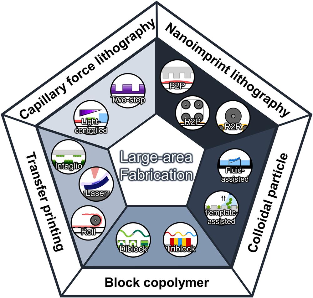
This review examines unconventional micro/nanofabrication methods that satisfy low-cost and high-throughput requirements and highlights their ability to fabricate large-area submicrometer structures uniformly (Fig. 1). First, we describe soft lithography and its types, along with the characteristics of each method. In addition, based on the advantages of soft lithography, the high-throughput production of practical photonic devices is discussed. Specifically, soft lithography achieves high throughput and scalability through simple processes using stamps. Further, colloidal photonic crystals and block copolymer (BCP) self-assembly approaches using the assembly of small molecules are classified in terms of various types of self-assembly methods based on their fundamental principles. In addition, their potential for use in large-area fabrication as well as controlling the shape and dimensions of structures using different assembly methods is discussed. Finally, we present limitations of each method and an outlook on the future direction and potential of nanofabrication.
Sign up for Photonics Insights TOC. Get the latest issue of Photonics Insights delivered right to you!Sign up now
2 Soft Lithography
Micro/nanofabrication techniques have been extensively used to engrave nanopatterns for constructing photonic devices. However, conventional micro/nanofabrication techniques such as FIB lithography, EBL, and scanning probe lithography (SPL)[29,30] are time consuming and expensive. Furthermore, EBL and SPL require complex proximity-correction processes to compensate for light distortion for the case where the desired patterns are smaller than the wavelength scale of the photons. Thus, these challenges need to be addressed to facilitate the use of these techniques in applications related to sub-wavelength nanostructures, such as large-area patterning and curved surfaces[31,32].
Soft lithography has emerged as a novel technology owing to its capability of patterning on flexible large-area substrates. It can fabricate or replicate submicrometer structures using elastomeric stamps, most notably polydimethylsiloxane (PDMS). It facilitates high-throughput manufacturing as it involves simple processes (molding, stamping, etc.) and low-cost organic/polymeric materials, and the stamps can be reused. This section discusses various types of soft lithography techniques and demonstrates their potential for practical applications.
2.1 Nanoimprint Lithography
Nanoimprint lithography (NIL) is a low-cost, high-throughput, and high-resolution patterning method that involves the use of a soft stamp. It has been actively researched by using various materials[33–37] and combining with different fabrication methods[38]. In NIL processes, a stamp consisting of inverse patterns replicates the desired patterns on a substrate by curing the resist with ultraviolet (UV) or heat. This technique can be classified based on two aspects: (i) resist curing and (ii) contact type.
2.1.1 NIL variants based on resist curing
NIL is categorized as thermal NIL and UV NIL, depending on the triggers of resist curing. UV NIL involves the use of a photopolymer resist, whose curing trigger is UV light [Fig. 2(a), i]. A typical UV NIL process is described as follows. A resist is spin-coated onto a substrate, and a stamp with an inverse shape of master mold patterns is created using PDMS. Owing to the stamp being in contact with the resist, it is filled with the resist under the desired pressure and time. Subsequently, the resist is hardened via UV exposure at room temperature. Consequently, the stamp is released, and the patterns are transferred to the substrate. UV NIL offers certain advantages over thermal NIL in terms of productivity because it can be performed at room temperature and in low-pressure conditions.

Figure 1.Large-area, low-cost fabrication methods are introduced as follows: nanoimprint lithography, transfer printing, capillary force lithography, block copolymer self-assembly, and colloidal photonic crystal self-assembly.
Figure 2.Types of nanoimprint lithography (NIL) depending on curing stimuli and contact types. (a) NIL variants based on resist curing. (i) NIL processes using a photopolymer resist, whose curing trigger is UV light. (ii) NIL processes using a thermoplastic polymer resist, whose curing trigger is heat. (b) NIL variants based on imprint contact types. (i) P2P NIL processes through contact between flat stamp and substrate. Reprinted with permission from Ref. [41], copyright 2021, American Chemical Society. (ii) R2R NIL processes using a pattern roller. Reprinted with permission from Ref. [45], copyright 2015, American Vacuum Society. (iii) R2P NIL processes through contact between rollers and flat substrate. Reprinted with permission from Ref. [47], copyright 2022, Multidisciplinary Digital Publishing Institute.
Thermal NIL, known as hot embossing, uses a thermoplastic polymer resist that softens when heated [Fig. 2(a), ii][39,40]. A thermal NIL process is conducted at a stamp temperature higher than the substrate transition temperature of the resist. The elevated temperature and sufficient pressure provide fluidity for the resist, which facilitates its entry between the patterns of the stamp. Thereafter, before detaching the stamp, the imprinting temperature is lowered below the resist temperature to allow its solidification, which leads to pattern transfer.
2.1.2 NIL variants based on contact types
NIL can be categorized based on imprint-contact types. Three contact types for the NIL process are possible: plate-to-plate (P2P), roll-to-roll (R2R), and roll-to-plate (R2P) NIL. In this paper, we describe these methods, including their overall configurations and applications.
In P2P NIL, imprinting proceeds through contact between the flat stamp and the substrate [Fig. 2(b), i][41]. Recently, a study realized 30 nm features using the P2P method, thereby indicating the potential of high-resolution patterning in NIL[42]. This method is independent of the size of the contact area because it enables the use of a stamp having the same area as the total pattern area of large-area micro/nanostructures. However, some force is required to increase the imprint pressure as the contact area expands. In addition, if the resist is deposited using the drop method (instead of spin-coating), which results in direct absorption of the resist into the stamp, air is readily trapped between the stamp and substrate. This leads to defects in the imprinted outcome. Hiroshima et al. demonstrated a solution to these bubble defects using pentafluoropropane based on gas condensation[43,44]. They proposed two methods, namely, resin squeezing, which discharges bubbles from the mold, and gas condensation, which significantly decreases the volume of the bubbles.
R2R NIL uses a pattern roller consisting of inverse patterns to imprint patterns onto a flexible substrate on support rollers [Fig. 2(b), ii][45]. Considering the factors of high speed and large area, roller-based imprinting processes capable of continuous production have been proposed. R2R NIL differs from P2P NIL, which has difficulties in applying uniform pressure to the mold and ensuring uniformity in the residual layer of the resist owing to the large contact area. The contact area between the rollers and substrates on the support rollers is smaller than that of the P2P NIL. This results in a reduced imprinting force and allows to realize a continuous process, thereby facilitating large-area patterning. In addition, because the process continuously patterns a large area by spinning reusable rollers, R2R NIL is a cost-effective technology for the mass production of nanostructures[46].
R2P NIL follows a process similar to that of R2R NIL, except that the patterning roller transfers the patterns to the substrate [Fig. 2(b), iii][47]. Roller-based methods have realized sub-100 nm features; however, the fabrication of sub-50 nm nanostructures is challenging because of the requirement of precise contact angle control between the resist and substrate[48]. These methods also use the continuous resist coating mechanism rather than the spin-coating of the resist, which is mainly used in P2P NIL. However, the mechanism is more complicated and requires uniform control.
2.1.3 Applications of NIL
NIL can be used to fabricate uniform nanopatterns on any flexible substrates through a single-step process. This technology has also been investigated for use in realizing industrial-scale applications that require mass production with low-cost materials, mask-free processes, low manufacturing cost, and high production speed[49,50]. The polymers mainly used in NIL have wide applicability in optical/electronic devices such as 3D imaging[51], solar cells[52,53], light-emitting diodes (LEDs)[54], and polarizers[55,56] because of their ease of manufacturing, low cost, and low reactivity. In addition, NIL has been researched for fabricating metasurfaces using metals such as gold (Au)[57]. Thus, the feasibility of various materials in NIL has been expanded to other application fields. We confirmed the characteristics of NIL in terms of high resolution, scalability, productivity, and facileness via antireflective films[58], polarizers[59], solar cells[60], and metaholograms[61].
The scalable fabrication of antireflective flexible films has been realized via thermal R2R NIL, and processing parameters (e.g., web speed and temperature) have been investigated[62]. Jacobo-Martín et al. achieved the desired optical performance covering ranges of 400–700 nm by realizing sub-wavelength scale moth-eye structures via R2R NIL [Fig. 3(a), i and ii][58]. The processes are carried out at pressure set to a value of 0.2–0.3 MPa and temperatures ranging from 80°C up to 140°C. Furthermore, they defined a correlation between the process parameters with the optical and mechanical properties of the films, proving the optimization of thermal R2R NIL. Also, Ok et al. showed a dual-band infrared (IR) filter covering ranges of 6–8 and 10–12 µm by patterning a sub-wavelength scale metal disk array via UV R2R NIL. They demonstrated that R2R NIL continuously fabricates large-area micro/nanostructures on flexible substrates at high speed and low cost.
Figure 3.Various applications using the NIL. (a) (i) Thermal R2R NIL for an antireflective film. The processes go on under a certain range of pressure (P) and temperature (T). (ii) Measured total reflection spectrum. (iii) Scanning electron microscope (SEM) image of imprinted moth-eye structures at 140°C. Inset: 3D reconstructions of atomic force microscope (AFM) images of imprinted areas. Reprinted with permission from Ref. [58], copyright 2021, Springer Nature. (b) (i) P2P NIL for an infrared nanowire grid polarizer. (ii) TM and TE transmittance spectrum. (iii) Photograph of the polarizer with 4-inch area. Reprinted with permission from Ref. [59], copyright 2018, Optica. (c) (i) Schematic of the P2P NIL for solar cells with grating structures. (ii) Power–voltage graph of solar cells with/without grating structures. (iii) Side view of the SEM image of grating structures via imprinting with vibration. Reprinted with permission from Ref. [60], copyright 2022, Elsevier. (d) (i) P2P NIL using particle-embedded resist (PER) for metasurfaces. (ii) Calculated hologram efficiency. (iii) Simulated/generated holographic images of metasurfaces. Reprinted with permission from Ref. [61], copyright 2019, American Chemical Society.
With polarization imaging and spectral analysis, IR polarizers have attracted attention in IR optics and nanofabrication. Conventional IR polarizers are mainly made by depositing nanometallic wires on IR-transparent materials such as KRS-5 and . However, these materials are brittle and hygroscopic, built on hard substrates, and are less compatible with curved compositions. Therefore, a flexible polarizer brings significant progress for applications including displays, monitors, etc. Kang et al. realized flexible 4-inch (1 inch = 2.54 cm) polarizers using thermal NIL [Fig. 3(b), i and iii][59]. They demonstrated the polarization characteristics, showing TM transmittance greater than 70% in wavelength ranges of 4.70–5.69 and 5.75–6.59 µm [Fig. 3(b), ii]. Also, an extinction ratio of more than 20 dB in the wavelength range of 3.6–6.7 µm is exhibited, implying great polarization characteristics. Furthermore, they emphasized functionality of the flexible IR nanowire grid polarizer due to applicability in the fields of curved surface monitoring equipment and polarized imaging equipment.
There has been growing interest in solar energy as an ideal green energy source. However, its low power generation efficiency and high cost are significant obstacles in photovoltaic technology. Gu et al. fabricated Si solar cells using vibration-assisted UV NIL [Fig. 3(c), i and iii][60]. They developed NIL by applying vibration to the conventional method of imprinting, which can improve the filling rate of photoresists by 25% and give higher pattern accuracy. Through this method, they realized periodic nanogratings, showing power conversion efficiency (PCE) increased by 25% when compared to bare Si solar cells [Fig. 3(c), ii]. Also, textured surfaces enhance light collection, realizing efficient light modulation including reflection control and light trapping properties[63]. This modulation has been investigated to enhance the efficiency of a solar cell by texturing at the front of the solar cell or using pre-textured solar cell substrates[64,65]. Amalathas et al. fabricated periodic inverted nanopyramid structures in monocrystalline Si solar cells[66]. They realized nanostructures uniformly over a large area of through two UV imprint processes. This implies that NIL is a scalable and low-cost fabrication method that eliminates defect generatability due to etching. Thereafter, employing such structures, an improved PCE of 11.73% is achieved by reducing Fresnel reflection and trapping incident light into the solar cells.
Metasurfaces comprising periodic sub-wavelength nanoantennas have overcome the miniaturization limitation. Also, various materials such as [67], perovskite[68], and silicon[69] have been studied for metasurfaces to realize various functions, and many manufacturing methods are being developed to reach nanoscale feature sizes and high resolution. Consequently, they have been applied to metalenses[70], metaholograms[71], and color printing[72]. However, the use of EBL and holographic lithography to realize large-area metasurfaces has led to high manufacturing costs and optical diffraction limit problems such as a proximity effect[73]. Kim et al. proposed UV NIL as a one-step printable platform without secondary operations (e.g., etching and deposition), demonstrating the feasibility of NIL for the mass production of optical metamaterials [Fig. 3(d), i][61]. This one-step process facilitates high productivity and low cost in the fabrication of optical devices. In addition, using a UV-curable particle-embedded resist, the refractive index of the resist itself is increased, which enables the use of the patterned resist as a metasurface. The fabricated metaholograms exhibit a conversion efficiency of 46% for , which is comparable to that of low-loss dielectric metasurfaces [Fig. 3(d), ii and iii].
Palladium (Pd)-based sensors have the potential for reversible gas-sensing capabilities and sensor mechanisms owing to their light weight and mechanical durability[74,75]. However, as Pd structures become smaller and the surface area becomes larger, high resolution is required. Lim et al. demonstrated scalable UV NIL fabrication processes with a polycarbonate (PC) film through the fabrication of flexible and durable gas sensors[76]. In addition, they showed that sensors with a size of maintain sensing performance with a response time of 57 s at 50 ppm (parts per million) concentration and achieve 3500 ppm of with a fast response time of 18 s.
2.2 Transfer Printing
Transfer printing is an emerging technique for deterministic assembly of nanomaterials into functional arrangements. It involves transferring patterns onto a target surface from a donor via a stamp. The typical process comprises peeling-off and printing steps. Desired structures on the donor substrate are first picked up onto a stamp, which is then transferred onto the target substrate after the stamp contacts the target substrate. The stamp used in both the pickup and printing steps is crucial for the successful implementation of the transfer printing process with high fidelity and easy control. This method is primarily dependent on the interfacial adhesion between the donor substrate/film, film/stamp, and film/target substrate. Therefore, the adhesion strength and peeling velocity are important variables in the transfer printing process. This method exhibits the properties of uniformity, reproducibility, and scalability. Consequently, it has been used in the fabrication of high-quality stretchable devices such as wearable bio-integrated electronics[77,78] and chemical sensors[79] compatible with various materials of a printable layer, demonstrating its potential for high-throughput and practical use. We introduce three modified types of existing printing processes among various types of transfer printing methods: intaglio, laser-driven, and direct roll transfer printing.
2.2.1 Intaglio transfer printing
Intaglio transfer printing uses an intaglio trench, which is a plate engraved in the shape of the desired patterns, to transfer the patterns onto the target substrates. Previous printing methods exhibit discrepancies between the original designs and transferred patterns owing to interfacial adhesion. Although existing transfer printing can be compatible with various materials, it fails to offer high-resolution/quality patterning. Kim et al. proposed a novel reverse-offset printing technology by patterning sub-10 µm copper nanowire (CuNW) transparent conducting electrodes[80]. The intaglio trench allows only the desired pattern to remain on the stamp, without any morphological changes [Fig. 4(a)]. In addition, the method ensures high-resolution aligned pixels through multiple transfer printings, thus realizing that the sheet resistance of the CuNW micropatterns decreased to as the irradiation energy increased to . The ability to transfer patterns on various substrates regardless of the size, shape, and arrangement of pixels results in high-performance operation and miniaturization of the devices, coupled with several application possibilities[81]. Also, Choi et al. proposed an intaglio transfer process integrated with quantum dots (QDs) to create high-resolution full-color RGB QD LED (QLED) arrays, realizing a high electroluminescence performance of 14,000 cd m−2 at 7 V[82].
Figure 4.Mechanisms of different transfer printing methods. (a) Transfer printing processes using an intaglio trench, which allows only the desired pattern to remain on the stamp without any morphological changes. Reprinted with permission from Ref. [80], copyright 2022, American Chemical Society. (b) Laser-driven transfer printing processes. Selectively heating the inks via laser induces strong thrust between stamp and inks, forming a pattern on receiver. Reprinted with permission from Ref. [83], copyright 2021, John Wiley and Sons. (c) Direct roll transfer printing processes. Si nanoribbons (NRs) are released by undercut etching of the buried oxide (box) (scale bar 10 µm, red line), and then brought into direct contact with semi-cured polyimide (PI) thin film (scale bar 25 µm, black line). Reprinted with permission from Ref. [85], copyright 2021, Springer Nature.
2.2.2 Laser-driven transfer printing
In transfer printing, the transferred patterns are significantly influenced by the interfacial adhesion strength, which is dominated by van der Waals interactions. The key role in the transfer process is to regulate interfacial adhesion states between strong for pick-up and weak for printing in a repeatable manner. Conventional pick-up and transfer processes proceed in vacuum chunks, but the size of the structure is sub-100 µm, and the limit to reduction of the vacuum system still remains a great challenge. Luo et al. presented an advanced transfer printing technique based on thermally controlled tunable adhesives[83]. The thermally controlled tunable adhesive provides desired adhesion states in transfer processes [Fig. 4(b)]. The inks successfully attached to the adhesive of the stamp are selectively heated via a laser beam. This process causes interfacial delamination to form patterns on a target substrate owing to the strong thrust strength. By changing 100°C temperature, suction strength of 25.5 kPa and thrust strength of 32.8 kPa are offered. They demonstrated that the thermally induced air pressure change in the cavity facilitates interface bonding/debonding.
In addition to the thermal control method, a way to change the adhesion state through the unique structure of the stamp was also proposed[84]. Kim et al. studied pressure-modulated adhesion using a stamp with four features of pyramidal relief. The structures control the adhesion strength such that the strength is reversibly switched when the stamp peels off the ink from the donor and transfers the ink to the target substrate. Here, a method using surface relief structures, developed to control the modes of adhesion and observed in geckos, is discussed. When an object is brought from the donor, the adhesion strength is maximized by increasing the contact area through the collapse of the regions between microchips. Subsequently, the elastic restoring force causes the stamp to return to its original shape, gripping the object only at the sharp points of the microtips. Consequently, the adhesion strength is minimized, and a high peeling-off velocity is promoted when transferring objects from the stamp to the target substrate. These characteristics enable rapid, reliable, and repeatable transfer printing, which indicates high productivity and potential for application.
2.2.3 Direct roll transfer printing
Many advances in transport printing have been made for large-scale implementation of high-quality nanostructures. Zumeit et al. proposed the direct roll transfer printing as a single-step process without using any elastomer stamp [Fig. 4(c)][85]. Conventional transfer printing has difficulties in controlling mechanisms of viscoelastic PDMS stamps for transferring sub-100 nm thick structures. Direct roll printing avoids the use of PDMS stamps, thus reducing the complexity of processes. Si nanoribbons (NRs) are brought into direct contact with semi-cured polyimide (PI) thin film, which enhances the adhesion between NRs and receiver substrates during imprint. Also, lower process steps, shorter printing time, enhanced printing yield, and lower fabrication cost are realized compared with the conventional approach. They demonstrated the high transfer yield of with perfect registration, showing the possibility of printing ultrathin micro/nanostructures based on other high-mobility materials. The printed Si NRs were used as channel materials to obtain high-performance transistors, showing great mobility [>630 cm2/(V·s)], current on/off ratio (∼106), and robustness after 100 cycles of bending.
2.2.4 Water-assisted transfer printing
The transfer of nanodevices onto diverse substrates such as papers, plastics, and glass has not been easily achievable before. As properties such as flexibility, transparency, biocompatibility, and conductivity of the substrates are required for diverse applications such as flexible displays[86] and transistors[87], technological developments have become necessary. Here, water-assisted transfer printing methods have been proposed to overcome the difficulty in transferring multiple layers onto unconventional substrates. In addition, the method proceeds with each layer aligned at approximately 100% while maintaining the measured efficiency of the transferred devices. Peeling-off proceeds in a water bath at room temperature based on the phenomenon of water penetrating the interface between the peeling layer and donor[88]. This process occurs in 3–4 s, following which the nanowire electronics are transferred to the target substrate. The transfer of a 4-inch wafer-scale area of microelectrodes is demonstrated, implying the scalability of transfer printing. In addition, this method offers certain advantages, such as insensitivity to mechanical and thermal stresses on the target substrate and the feasibility of diverse nonconventional substrates.
2.2.5 Applications of transfer printing
Flexible electronic systems, including wearable devices, have been actively investigated because they can be bent, folded, and stretched without degrading their electrical performance and reliability. Here, transfer printing has been extensively studied as a technology for integrating functional devices with flexible substrates[89,90]. Wide-ranging applications have emerged owing to the ability of the transfer printing method in enabling the assembly of functional devices onto flexible or specific-shape (e.g., curved) substrates such as polyethylene terephthalate films and PI substrates[91,92]. The demonstrated functional components include transistors[93,94], capacitors[95], LEDs[96,97], energy-harvesting devices[98], and various sensors[99].
Stretchable solar cells have been employed as wearable power generators because of their robust mechanical properties, which are vital for portable electronic devices[100]. However, solar cells are unsuitable for stretchable systems because of their intrinsic rigidity and brittleness. To overcome these constraints, transfer printing is required, which involves arranging an inorganic semiconductor from a donor to a stretchable substrate. However, the transfer printing of inorganic amorphous thin-film semiconductors is challenging owing to the absence of a suitable sacrificial layer. Nam et al. developed a novel approach using a water-soluble sacrificial layer[100]. Stretchable inorganic amorphous thin-film solar cells were fabricated via transfer printing with a sacrificial layer, which is placed on the donor and patterned upon. When peeling off the pattern using a stamp, the sacrificial layer weakens adhesion, thereby allowing successful transfer. Owing to the layer requiring mild etching conditions, compatibility with high process temperatures, and mechanical stability, the transfer printing of the solar cells over a large area was realized. A comparison of the performances of the solar cells before and after transfer printing revealed that the etching or transfer printing process has no effect on their performance, as shown by the current density–voltage characteristics. This demonstration of stretchable solar cells with inorganic amorphous thin-film semiconductors significantly broadens the applications of solar cells as well as the capabilities of transfer printing.
Metallic nanogaps have many applications in nanoscale photonics and electronics. Nanostructures with metallic nanogaps can confine the electromagnetic field within the deep-sub-wavelength region of the gap and control/enhance the fluorescence emission. This enhancement is suited for optical systems such as surface enhanced Raman scattering (SERS) and IR sensing. Chen et al. enabled the fabrication of multiscale metallic nanogaps with reduced gap size ()[101]. They overcome the resolution limitations of direct lithography approaches by transferring Au ink onto PDMS [Fig. 5(a), i]. After transferring the Au ink with large gap size of 120 nm to the pre-stretched PDMS, retrieving the PDMS reduces the gap size to 5 nm. They evaluated the photoluminescence (PL) enhancement by transferring again onto flakes. Compared to the PL of flakes decorated with a 120 nm gap (orange line), the post-assembled metallic nanogaps led to enhanced PL emission (red line) [Fig. 5(a), ii]. By realizing sub-10 nm metallic nanogaps in two transfer printings, they showed a wide variety of applicability including sensing, imaging, and energy applications.
Figure 5.Various applications of transfer printing. (a) (i) Transfer printing integrated with post-assembly to fabricate the sub-10 nm nanogap. A gold nanodimer with 120 nm gap size is transferred onto pre-stretched polydimethylsiloxane (PDMS) substrate, which then is released. After releasing the substrate, the large gap in dimer is shrunk (). (ii) Photoluminescence (PL) spectra of MoS2 flake with the post-assembled nanodimer (red line) and initial nanodimer (orange line). (iii) SEM images of gold nanodimer before and after releasing the stress. Reprinted with permission from Ref. [101], copyright 2020, John Wiley and Sons. (b) (i) Synthesizing and transfer printing processes of ZnO nanostructures on a polycarbonate (PC) substrate. (ii) Transmittance spectra of A series and B series. A series represents as-grown nanorod arrays, and the corresponding transferred nanorod arrays with 60 s O2 treatment are represented as B series. Inset: SEM images of transferred nanorod arrays. Reprinted with permission from Ref. [109], copyright 2022, John Wiley and Sons.
LEDs have the potential to efficiently use energy for applications in flexible electronic devices. Recently, gallium nitride (GaN)-based LED devices, which have been used in liquid crystal displays, lighting devices, etc., have been studied for high-efficiency and high-quality light sources[102–104]. Blue InGaN LEDs are used as alternatives for the existing infrastructure under general illumination[105]. Kim et al. fabricated a thin, flexible, and white-light module by fabricating the phosphor in PDMS and laminating it via tape to a matching array of microscale inorganic LEDs (μ-ILEDs). Transfer printing demonstrated that the assembly of LEDs could be easily attached to plastic or glass substrates at room temperature while maintaining performance, such as emission intensity.
To effectively modulate the phase and wavefronts of light, metasurfaces comprising periodic sub-wavelength nanostructures have been exploited as holograms, lenses, color filters, reflectors, etc.[106–108]. Specifically, in color filters, several colors are obtained by tailoring the structural parameters associated with the nanostructures. Moreover, the incoming light can be filtered into distinct colors according to the structural parameters of the nanostructures. Liu et al. demonstrated the scalability of the transfer printing process through the fabrication of “windmill” ZnO patterns including more than 300,000 nanorod units on PC film [Fig. 5(b), i and iii][109]. Further, to overcome the adhesion strength between the structures and target substrates, poly(methyl methacrylate) (PMMA) was chosen as the protection and transfer layer because of its high Young’s modulus () in the solidified PMMA polymer. Although there was a variation in the GaN layer interference on the substrate before and after the transfer, measured spectra showed that the major peaks of the spectrum curves are redshifted with the increase in the diameter of the nanorods [Fig. 5(b), ii]. In particular, for the transferred arrays, the lowest transmittance constantly decreases with the change in the diameter of the nanorods, implying a high color filter efficiency. In addition, they demonstrated that the presented color pallets indicate full coverage of the color gamut, indicating successful transfer printing.
2.3 Capillary Force Lithography
Capillary force lithography (CFL) is a novel technology that improves productivity through process simplification and process time/cost reduction. Owing to the use of complex nanostructures in photonic devices and electronics, many patterning techniques are required to produce scalable, uniform structures in a facile and reproducible manner. Further, techniques such as EBL, ion-beam lithography, dip-pen lithography, BCP lithography, and CFL[110,111] have been developed to overcome the limitations of large-area fabrication of submicrometer structures.
If the polymer film is thin and the interaction between films and substrates is weak, the polymer fills the void space of the stamp without any applied pressure. Consequently, the existing force (e.g., pressure) used for molding the polymer is changed to a capillary force; the patterning technique using this force is referred to as CFL. This section briefly classifies the different types of developed CFL and demonstrates the applicability of CFL, introducing its various practical applications.
2.3.1 Light-controlled CFL
Recently, many studies have been conducted to spatially modulate the nanopixel’s height[112,113]. To enhance functionality through this, grayscale photolithography and scanned beam lithography are used for fabrication of nanostructures. However, the methods have high production cost due to complex processes. Li et al. reported that height-controlled CFL is possible with certain photopolymers[114]. Since it is difficult to control the polymer’s capillary rise to realize a grayscale nanopixel with conventional CFL by itself, they introduced light-controlled CFL [Fig. 6(a)]. The photopolymer spread to the substrate is irradiated with different UV doses to adjust the thickness of the polymer layer. At this step, the polymer layer’s top portion cures partially, forming an ultrathin liquid-phase polymer layer on the solidified bulk. An increase (decrease) in UV dose leads to a decrease (increase) in the liquid layer thickness. Then, the elastomeric nanocavity array and the partially cured polymer are contacted, generating a capillary force. Consequently, the capillary rise occurs until the liquid-phase layer has been solidified completely, enabling to control the height of nanoposts in the range of 5–8 nm. This mechanism shows significant potential for high-resolution, 2D patterned grayscale CFL due to the nature of light.
Figure 6.Developments in capillary force lithography (CFL) methods. (a) Optically height-controlled CFL processes. A UV-curable polymer, NOA73, is precured by UV irradiation with different UV doses for each of the four division areas. This leads to thickness difference of the liquid-phase photopolymer layer (scale bar 1 µm). Reprinted with permission from Ref. [114], copyright 2020, American Chemical Society. (b) Continuous fabrication processes via two-step CFL. Polyurethane acrylate (PUA) resin is partially cured by UV irradiation, and top portion of the resin is completely cured with pressure.
2.3.2 Two-step UV-assisted CFL
Micro/nanoscale hierarchical structures aid in the advancement of diverse photonic[115,116], electronic/optoelectronic devices[117,118] as multiscale structures improve structural functionalities compared to single-scale structures. Soft lithography approaches offer an efficient solution for the fabrication of high-quality micro/nanoscale hierarchical structures[119,120].
Jeong etal. proposed a two-step UV-assisted CFL for fabricating monolithic micro/nanoscale structures over a large area ()[121]. They found that a partially cured microstructure can be further molded by sequential nanopatterning, which results in a monolithic hierarchical structure that enhances mechanical strength and chemical stability. As the fluidity of the upper part of the polymer must be adjusted well during the first molding, the appropriate curing time in the two-step UV-assisted CFL is an important factor. Later, for high fluidity, they described an improved version of CFL that involves partial curing and vacuum-assisted hydraulic filling for fabricating monolithic bridge structures[122]. In small-scale structures, capillary forces are dominant, causing fluid flow along the wall of the stamp. However, for a partially cured polymer, capillary forces are not sufficiently high to facilitate polymer movement through the long channels connecting the structures because of the low fluidity of the polymer. They addressed this issue by moving the polymer into the channels while decreasing the hydraulic pressure through a vacuum, forming bridge structures.
Lee et al. reported continuous partial curing and tip-shaped modification approaches with microscale mushroom-shaped structures [Fig. 6(b)][123]. Typical methods with mushroom-shaped structures are limited owing to the failure of tips during demolding. To solve this problem, they used two-step UV-assisted CFL, which includes partial curing and tip widening. Also, by integrating with the R2R process, a continuous process is realized to increase productivity without any defects. In addition, the shape and size of the structures can be tuned by changing the geometries of the molds. This facile molding technique can serve as an alternative for fabricating dual-scale polymer micro/nanoscale structures. Consequently, the versatility of CFL, such as partial curing of two-step CFL, has broadened the range of applications to nanoscale structures of different shapes.
2.3.3 Solvent-assisted CFL
A typical CFL process utilizes the capillary filling phenomenon of a molten polymer within the cavity of a stamp pattern at high temperatures to melt the polymer. Yu et al. proposed a solvent-assisted CFL[124]. This method uses a solvent to soften the polymer at room temperature. The PDMS stamp functions as a solvent tank; when it comes into contact with the polymer, the stored solvent diffuses into the polymer, causing it to dissolve. Subsequently, the capillary force drives pattern formation. They tuned highly regular and reproducible micro/nanoscale polymer patterns with stamps by modulating the experimental conditions. Moreover, owing to the fast and large-area patterning ability, complex patterns also are easily fabricated using this method. In addition, this method enables the cross-patterning of polymer and organic devices without degradation.
2.3.4 Applications of CFL
The versatility of CFL has facilitated its applications in optical research[125,126]. In particular, remarkable features such as reusability of stamps, compatibility with various large-area substrates, and facile molding have realized complex structures. Using these structures, practical applications such as delivery systems[127] and SERS[128] have been demonstrated.
With the evolution of displays to ultrahigh definition (UHD), the number of pixels per inch has increased, requiring high technologies such as high density of pixels and high precision in fabrication. Conventional methods render the fabrication of μ-LEDs for compact UHD displays challenging because of their high fabrication cost/time and complicated processes. In particular, patterning processes with secondary operations, such as etching and deposition, cause system complexity. Here, we discuss CFL capable of achieving the controlled surface pattern with high precision and morphology of organic materials. Kim et al. fabricated micro-perovskite LEDs (μ-PeLEDs) for low-cost and large-area μ-LED applications, as perovskites are managed via simple processes at low temperatures [Fig. 7(a), i][129]. PeLEDs are suitable for display applications because they exhibit greater luminescence efficiency than conventional LEDs[130]. However, due to the long diffusion length of excitons, PeLEDs have low external quantum efficiency (EQE). To solve this problem, the pixel size should be reduced by using a micro-patterning approach having fewer defects. They demonstrated that CFL reduces the pixel size on a 10 µm scale. They also realized μ-PeLEDs, which exhibit an EQE of 5.9% at 4 V by forming uniform pattern arrays and confirmed the performance of devices based on poly(ethylene oxide) concentrations [Fig. 7(a), ii and iii].
Figure 7.Various applications of CFL. (a) (i) Perovskite patterning method using CFL. (ii) External quantum efficiency (EQE) spectra of micro-PeLEDs with 0.06%, 0.08%, 0.10%, and 0.12% (mass fractions) poly(ethylene oxide) (PEO). (iii) Light-emitting images of the micro-PeLEDs with 0.06% and 0.10% PEO. Reprinted with permission from Ref. [129], copyright 2022, Elsevier. (b) (i) Ag nanowire (AgNW) solution patterning using CFL. Hydrogel infiltrated at the edge of the PDMS stamp is cured on the patterned AgNWs by UV irradiation, and then washed off by ethanol. After ethanol washing, hydrogel-free AgNWs remain. (ii) Gauge factor as a function of applied tensile strain. (iii) Field emission SEM image of the patterned AgNWs on glass. Reprinted with permission from Ref. [131], copyright 2017, American Chemical Society.
As flexible strain sensors are used to monitor kinetic motions and act as on-skin electronics, high flexibility, response/recovery speed, and durability of sensors are important key factors. Also, an electrode material used on capacitive strain sensors should be chosen properly. Ag nanowire networks (AgNWs) are considered as one of the most promising materials for deformable electrodes. Lift-off lithography and laser printing are mainly used to pattern AgNWs; however, these methods have drawbacks such as limited patterning shapes and high production cost. To solve them, Kim et al. proposed patterned AgNWs using CFL as an alternative patterning technique[131]. They progressed the CFL using the AgNW solution and embedded it in PDMS to complete the capacitive strain sensor [Fig. 7(b), i and iii]. AgNW solution is spin-coated on the glass substrate, and then annealed. After annealing and cooling, AgNWs are patterned using a PDMS stamp by CFL. The UV-curable hydrogel solution is dropped at the edge of the PDMS stamp, infiltrating space between the AgNW film and PDMS stamp. After a curing hydrogel, the cured hydrogel patterns on the AgNWs are washed off in the ethanol bath. Consequently, a pattern of hydrogel-free AgNWs remains. As a result of applying tensile force through the completed sensor, they proved that capacitance decreased as the tensile increased, showing a gauge factor of , which is larger than the gauge factor limit of one for the typical parallel-plate capacitive strain sensor [Fig. 7(b), ii]. The gauge factor is defined as GF = ΔC/C0 (, capacitance; , strain). They showed the development of the elastomeric substrate with elastic deformation as well as an improvement in electrical conductivity of AgNW anodes while maintaining high optical transparency.
Hydrogen gas sensors and hydrogen gas have been actively investigated as promising clean energy alternatives[132,133]. Specifically, the absorption of hydrogen on Pd has been studied in terms of changes in mass, volume, and electrical/optical properties[134,135]. These changes occur during the diffusion of hydrogen into Pd via the formation of a Pd hydride, which can be utilized in gas sensors to detect hydrogen. Pd-based sensors have been proven to exhibit high detection speed and high sensitivity[136]. Zou et al. demonstrated that CFL in combination with a polymer “grafting to” approach facilitates derivation of linear assembles of Pd nanocubes for large-area sensors[137]. In addition, the performance test of the sensor showed that the resistance increases at hydrogen gas concentrations between 0.3% and 3%, below which no response is observed, thereby demonstrating high sensitivity. This allows easy access to a self-assembly platform when fabricating large-area micropatterns. Moreover, these results indicate the possibility of fabricating nanodevices and commercializing the fabrication of devices using CFL.
3 Colloidal Self-Assembly
Photonic crystals are materials composed of periodic dielectric, metallo-dielectric, or even superconductor structures. By controlling certain parameters of the photonic crystal, such as periodicity, shape, and size, light with a certain wavelength range can be blocked. In addition, the refractive index in each direction can be varied depending on the periodicity of the photonic crystals in the spatial direction. Many photonic applications have been proposed such as waveguides[138,139], metasurfaces[140,141], displays[142], optical fibers[143], and sensors[144,145]. Sub-wavelength photonic crystals can be fabricated over a large area via colloidal self-assembly. In this section, we introduce colloidal self-assembly, various self-assembly methods, and their applications.
3.1 Colloidal Particles
Colloidal particles are solid particles suspended in a fluid and used to create a well-arranged structure on a substrate. Colloidal particles are synthesized via several methods, such as emulsion[146], dispersion[147], suspension[148], and the Stöber method[149]. These methods have facilitated precise synthesis of monodispersed colloidal particles such as silica[150], PMMA[151,152], polystyrene (PS)[153], Au[154], and silver (Ag)[155,156]. Moreover, these colloidal particles are able to form sub-wavelength photonic crystals.
3.2 Methods of Colloidal Self-Assembly
Nanoscale hexagonal close-packed (HCP) monolayer or multilayer structures are spontaneously established when the suspension is thermodynamically stable[157]. This implies that removal of the suspension induces packing of the colloidal particles[158]. The HCP self-assembled structure is used for photonic applications because of its sub-wavelength crystal size and periodicity[159,160]. For example, colloidal photonic crystals are formed via spin-coating[161]. Spin-coating is widely used in nanofabrication processes such as semiconductors[162,163] and metamaterial fabrication[164] owing to its rapid and easy-to-use characteristics. In the case of colloidal self-assembly, the relation between spin speed and thickness of wafer-scale monodisperse silica colloidal crystals[165] and the optimal conditions for the self-assembly of PS nanoparticles have been demonstrated[166]. In addition, various methods have been proposed such as convective self-assembly[167], the Langmuir–Blodgett (LB) method[168,169], the Marangoni effect[170], the template-assisted method[171–173], and the field-assisted method[174].
3.2.1 Fluid-assisted method
Fluid-assisted methods exploit the characteristics of fluids, such as surface tension, to induce capillary force[175] and the Marangoni effect[170,176]. Convective self-assembly involves a fluid-assisted process. Upon the movement of an upper blade coupled with the existence of a colloidal suspension, colloidal particles are self-assembled [Fig. 8(a)][177]. After a suspension is spread into the space between the blade and the substrate, the blade is withdrawn. Because the solvent evaporation induces a convective flow, the colloidal particles form arrays owing to the capillary force acting between them. For example, confined convective assembly has been demonstrated[167]. The colloidal suspension is positioned between the substrate and the blade that are connected to a machine, which controls the lift-up rate. When the blade moves, a meniscus is formed at the edge. Hot air is blown to evaporate water. The well-arranged particles are then fixed on the glass plate. Consequently, varying the lift-up rates and colloidal suspension concentration results in the formation of 2D or 3D structures.
Figure 8.Types of colloidal self-assembly techniques. (a) Fluid-assisted convective self-assembly. As the solvent evaporation induces a convective flow, the colloidal particles form arrays owing to the capillary force acting between them. (b) Colloidal self-assembly by using Langmuir–Blodgett method. By compressing the barrier, the monolayer is produced and then deposited on the vertically/horizontally positioned substrate. (c) Colloidal self-assembly by using Marangoni effect. Exposing a nanoparticle (NP)/ethanol (EH) suspension to a wet nitrogen (N2) stream induces the evaporation of EH and the condensation of water (H2O). This leads to the surface tension gradient [ and H2O ], driving the NPs/H2O toward the receding contact line. (d) Template-assisted self-assembly for plasmonic nanoarray. Photoresist is spread onto the antireflection coated (ARC) Si, and then imprinted to form a PDMS template. The template is used to align the colloidal plasmonic nanoparticles in a 2D square lattice. Right: SEM images of the fabricated master mold, PDMS nanohole arrays, and 2D plasmonic lattice. Reprinted with permission from Ref. [182], copyright 2019, American Chemistry Society.
Another fluid-assisted method is the LB method. An LB film, which is fabricated via the LB method, is an ultrathin film comprising arranged colloidal particles on a water surface [Fig. 8(b)]. Colloidal particles could form a densely packed thin film by compressing the barriers. When barrier compression occurs, a monolayer is produced and vertical/horizontal deposition occurs as the substrate is vertically/horizontally aligned. For example, well-arranged binary colloidal monolayers have been demonstrated[168]. The first step involves placing the wafer under water at a small angle to the horizontal plane. Colloidal particles then form well-arranged arrays at the air–water interface using a diluted ethanol solution. Monolayer structures of various shapes have been fabricated depending on the diameter ratio of the colloidal particles and the potential of the hydrogen (pH) value. The pH affects the contact angle between particles of different sizes, and high crystallization is achieved. Subsequently, various self-assembled structures are transferred to the target substrate through surface lowering. In addition, the LB method can induce colloidal self-assembly on the curved substrate such as flexible foil, bulbs, and optical cables with a simple process[169]. 600 nm silica nanoparticles are used as colloidal particles. Surface pressure depending on the area is investigated in isotherm conditions at each type of substrate. Also, the differences in the effective refractive index and transmission spectrum are observed between bare and PMMA composite films.
Although the LB method offers the advantage of manufacturing colloidal photonic crystals over a large area, it exhibits low mechanical instability. The Marangoni effect has been used to solve this problem[178]. It uses the movement of a liquid from a place with a low surface tension to a place with a high surface tension according to changes in the surface tension (the force that causes the surface of the liquid to contract itself to occupy as small an area as possible), which induces self-assembly. Nanoparticles/ethanol suspension is spread into a thin layer on the glass substrate, and then exposed to a stream of wet , which induces evaporation of ethanol and condensation of water [Fig. 8(c)][179]. This leads to a concentration gradient and the difference between the surface tensions of ethanol and water, driving the nanoparticles/water toward the receding contact line. Also, a Marangoni flow of ethanol carrying nanoparticles is induced toward the contact line and into the water. As the condensed water dries, the ordered nanoparticle array forms on the substrate. For example, large-area self-assembled nanosphere structures have been demonstrated[176]. The micro-propulsive injection method is used to create HCP structures. Subsequently, ethanol is added to the colloidal suspension to induce a surface tension gradient. When colloidal suspension is dropped on the air–fluid interface, surface tension induces the Marangoni force, and colloidal particles move until the entire surface area is covered by nanoparticle arrays. Consequently, high throughput is achieved, and the rapid fabrication rate and simple process facilitate its application to a large area and in various substrates such as rigid, flexible, and complex structures. In addition, a way to enhance the quality of colloidal self-assembly is demonstrated[180]. The conventional method uses sodium dodecyl sulfate (SDS) after emulsion is introduced at the air–water interface. SDS induces a lower surface tension gradient to reduce the defects of the structure. In contrast, the proposed method uses SDS pre-saturating water before introducing colloidal solution. Through the proposed method, a fabricated structure with fewer defects is observed.
3.2.2 Template-assisted method
Tailored substrates are fabricated via various lithography technologies. When colloidal particles slip on a tailored substrate, they are located on the patterned region by physical force. The tailored substrate used for this purpose is a template. Template-assisted methods contribute to further utilization of colloidal self-assembly by increasing design diversity. For example, template-assisted methods using physical and capillary forces have been demonstrated[181]. First, small holes are patterned via photolithography. Subsequently, a polymer bead dispersion is added between the top and bottom of the glass substrate. When the rear end of the bead dispersion is moved, capillary force is applied to the beads, and these move continuously unless confined in the holes. Various structures, such as monomers, dimers, triangles, squares, pentagons, hexagons, and double-layered structures, are achieved by controlling the ratio of the patterned hole diameter, depth, and bead diameter.
Template-assisted methods for plasmonic nanostructures have also been demonstrated [Fig. 8(d)][182]. The master mold and soft mold are fabricated based on laser interference lithography and UV-curable PDMS, respectively. The soft mold is used as the template. The colloidal Au nanoparticles are confined to the template by a guiding plate. The soft mold is used to align the colloidal plasmonic particles in a 2D square lattice. Consequently, the surface lattice resonance and localized surface plasmon resonance (LSPR) wavelengths are blueshifted when the strain increases (0% to 40%).
3.2.3 Field-assisted method
External electric or magnetic fields induce colloidal self-assembly by electromagnetic force[183–185]. During self-assembly, a uniform driving force minimizes defects. Although this method requires additional equipment setups, well-arranged self-assembly structures are formed with a uniform driving force. In the case of the electric-field-assisted method, 2D tunable self-assembled structures have been demonstrated[174]. Eight planar electrodes with the same height are used. For a uniform electric field, the gap between the electrodes and the substrate is controlled by varying the substrate thickness. Further, in the case of the magnetic-field-assisted method, self-assembly using the non-magnetic template method has been demonstrated[185]. The existing magnetic field-assisted method is not able to facilitate the arrangement of particles in the desired shape owing to the magnetic properties of the target substrate. This problem has been solved via the use of ferrofluids. The target patterned substrate is immersed in ferrofluid and modulated by magnetic-field-induced electromagnetic force.
3.2.4 3D structure method
Colloidal self-assembly also induces the formation of multiple layers or other complex structures. The layer-by-layer scooping transfer method has been demonstrated for multilayer structures[186]. A monolayer is formed at the air–water interface by floating colloidal particles. Consequently, a multilayer is realized by repeating the monolayer transfer process onto the target substrate. Similarly, multilayer structures with different particles have also been demonstrated[187]. The monolayer is first self-assembled on a hydrophilic petri dish. Following toluene vapor annealing, a mechanically stable monolayer is formed. If the same process is repeated for different particles, multilayer structures are formed, realizing complex shapes. For example, specific directional bonding structures have been demonstrated[188]. The structures are fabricated with deoxyribonucleic acid (DNA)-patched particles using a previously described method[158]. Patched DNA docks with other patched particles, and designed structures are formed. Subsequently, various bonding shapes, such as hybridized atomic orbitals, have been achieved.
3.3 Applications of Colloidal Self-Assembly
In the last decade, owing to advancements in colloidal self-assembly methods, many applications have been proposed, such as SERS[189,190], display[191], lithography technology[192,193], encryptions[194,195], sensors[190,196], and metamaterials[197,198]. In this section, we introduce various applications of colloidal self-assembly.
Through an analysis of the wavelength distribution of Raman scattering, the composition or bonding of a material can be determined[199,200]. When the Raman signal is intensified, material or bonding that is originally difficult to observe is seen; this intensifying method is SERS. Plasmonic nanostructures confine far-field light to a small volume[201,202]. If a small gap exists between plasmonic nanostructures, a highly concentrated electric field region occurs, which is referred to as a hotspot. The target should be positioned near the hotspot to intensify the Raman signal. Thus, SERS is widely used in molecular detectors[203,204], chemical technology[205,206], biomedical technology[207], and sensing[208,209].
Light is easily confined in a small volume with high-aspect-ratio nanostructures[210,211]. To exploit this advantage, scalable Au-attached silicon nanorods have been demonstrated[212]. After PS self-assembly, reactive-ion etching (RIE), and metal-assisted chemical etching are performed for the nanorod structures. The Raman signal of the target is significantly intensified by this SERS substrate. Even though nanostructures do not have a high aspect ratio, the Raman signal can be significantly intensified. For example, the SERS substrate is fabricated using the in situ patterning method [Fig. 9(a)][213]. Following the self-assembly of the colloidal monolayer on the substrate, RIE and Au deposition are performed to create a thin hole film. These nanostructures are then immersed in a Ag nitrate/sodium citrate solution and irradiated by LEDs. During irradiation, Ag particles are attached near the edge of the holes by the surface plasmons of the Au film. When the irradiation time is increased, the Ag area in the nanohole is enlarged. After taping out the Au film, the Ag nanostructures are fabricated [Fig. 9(a), i]. This substrate achieved a low concentration of various materials. Moreover, the Raman peak is varied depending on the LED illumination time (30, 60, 90, and 120 min) [Fig. 9(a), ii]. In addition, other large-area SERS substrates are demonstrated such as Ag, amorphous silicon multiple-layer-deposited structures[189], and 3D sunflower structure[214], which consists of Ag deposited silica and PS spheres.
Figure 9.Various applications of colloidal self-assembly structures. (a) (i) In situ chemical patterning processes for surface-enhanced Raman scattering (SERS) substrate. (ii) Raman spectra under different LED illumination times (30, 60, 90, and 120 min). Right: SEM images of the Ag nanoparticle array (scale bar 100 nm). Reprinted with permission from Ref. [213], copyright 2022, John Wiley and Sons. (b) (i) Multiple-patterning for a ring-shaped absorber. Right: SEM images after second polystyrene (PS) size reduction and PS removal. (ii) Absorption contributions of each TiN layer. Total power dissipation density of top ring-shaped TiN nanostructure (red line), bottom TiN layer (blue line), and the summation of two densities (black line). Reprinted with permission from Ref. [221], copyright 2021, Springer Nature. (c) (i) Colloidal self-assembly processes for anisotropic Janus structural color particles (SCPs) by phase separation and cardiomyocyte monitoring platform. (ii) Reflective peaks and reflection images of five different anisotropic Janus SCPs. (iii) SEM images of whole (black line, scale bar 100 µm), colorful hemispherical section (yellow line, scale bar 1 µm), and black oblate section (red line, scale bar 2 µm) of anisotropic Janus SCPs. Reprinted with permission from Ref. [225], copyright 2020, American Association for the Advancement of Science.
The refractive index and extinction coefficient are crucial factors affecting the efficiency of metamaterials[215]. For example, when a device has a high refractive index, it provides various sets of phase-dispersion space[216]. Although the refractive index is an important factor for modifying optical properties, it is limited in nature, ranging from one to three in the visible range[217]. Refractive-index-tunable metasurfaces have been demonstrated to overcome this limitation[197]. Au nanoparticles are self-assembled on a water surface. For well-arranged self-assembly, a proper volume ratio of hexane and toluene and an evaporation container are used. The self-assembled Au structures are then transferred to the PDMS substrate. The tunable refractive index and extinction coefficient are observed depending on the strains of the PDMS substrate in the visible and IR regions. In addition, other metasurfaces fabricated based on colloidal self-assembly with other materials such as silicon[218], selenium colloids[219], and titanium oxide ()[220] have been demonstrated.
Colloidal self-assembly contributes to anti-reflective coatings owing to its low-cost and scalable properties. For example, 3D hierarchical nanotowers have been demonstrated[198]. Nanotower structures are fabricated using colloidal particles and silicon substrate etching. Depending on the diameter, height, level, and material composition of the nanotower, the wavelength with near zero reflection is tunable. However, despite its tunability and near-zero reflection, the deviation of the reflection according to the wavelength is large. For a broadband range, scalable manufacturing of a near-perfect absorber has been demonstrated [Fig. 9(b)][221]. Most absorbers are composed of dielectric materials and metals that are used as gaps and reflectors, respectively. However, these materials are unsuitable for large-scale fabrication because of their high cost. Refractory metals have been used to solve this problem with their low cost and excellent mechanical and chemical properties. The fabricated structures are composed of top TiN rings and bottom TiN layers [Fig. 9(b), i]; therefore, the summation of the ring and layer absorption is the total absorption [Fig. 9(b), ii], and a result similar to that of the simulation is observed. The experimental results indicate significant absorption in the broadband region, visible to near IR.
In terms of easily creating 3D structures, colloidal self-assembly is able to contribute to structural color applications. Owing to their fadeless properties, structurally colored fibers have attracted attention[222]. The existing method of fabricating colored fibers has disadvantages because of the complicated processes and low controllability, but this problem is solved via colloidal self-assembly. For example, the facile fabrication of structurally colored fibers has been demonstrated[223]. The fabrication process involves lifting bare fibers from colloidal dispersion. The optical properties of the structurally colored fiber vary with the number of layers, which is controllable by the lift-up rate, size of the bare fibers, structural defects, and viewing angle.
Janus particles are patchy particles with different surface properties. Various Janus particles fabricated via colloidal self-assembly have been proposed. For example, transformable suprastructures have been demonstrated[224]. Poly(tert-butyl acrylate)-poly(3-triethoxysilyl)propyl-methacrylate is used to form Janus particles. Structure diversity is realized by separating self-assembly conditions, such as concentration, temperature, and sonication time. Due to structures of Janus particles, various structure colors can be achieved. The structure color resulting from phase separation has been demonstrated [Fig. 9(c)][225]. When co-assembled graphene oxide (GO) and silica colloidal particles are mixed and dropped, Janus particles are formed [Fig. 9(c), i]. These Janus particles have different optical properties depending on the colloidal particle diameters, which are caused by prohibition of certain wavelength light from total reflection or scattering [Fig. 9(c), ii]. In addition, owing to its anisotropic structure [Fig. 9(c), iii], when it flows in a fluidic channel, different moving distances are observed owing to the friction force difference between the Janus particles and nanosphere particles. These results indicate that Janus particles should be used in broader applications with flat substrates. Also, inverse opal structure fabricated by the proposed Janus particle can be used as a monitoring platform for target material.
Self-assembled colloidal structures have a photonic bandgap owing to the periodically arranged nanoparticles. Various structure color applications for displays have been proposed to exploit the advantages of colloidal self-assembly. For example, an inkjet printing patterning method for PS photonic crystal domes has been demonstrated[226]. The coffee-ring effect, which is a problem for the inkjet printing method, is solved by controlling the sliding three-phase contact line, which induces a high-aspect-ratio structure. When fluorescent molecules are inserted into the droplet, the fluorescence intensity is significantly intensified and a wide viewing angle is achieved. Moreover, these processes are compatible with PDMS substrates. Thus, the demonstrated structures should contribute to displaying pixels and flexible displays.
For high-efficiency displays, power enhancement using the layer-by-layer method has been demonstrated[193], where the floating layer is first self-assembled on the hydrophilic petri dish. After placing the substrate in the vessel, toluene vapor annealing is performed for mechanical stability. After repeating these processes, colloidal layers of different sizes are stacked. These layer-by-layer structures exhibit a high and wide band reflectivity property; therefore, it is used as a back reflector. Furthermore, the efficiency of the reflector-added LEDs is significantly enhanced compared with those of conventional LEDs.
4 Block Copolymer Self-Assembly
4.1 Block Copolymer
BCP consists of two or more polymers connected via linear covalent bonds. BCP spontaneously forms specific nanostructures through mutual attraction between blocks. Consequently, it has attracted much attention as an alternative to nanopatterning technology. For example, BCP self-assembly applications for semiconductor fabrication and inorganic (e.g., dielectric and metal) patterning have been proposed[227].
BCP is classified into diblock and triblock copolymers, depending on the number of blocks. Owing to the composition and bonding characteristics of BCP, phase separation occurs at specific temperatures and pressures. Upon the occurrence of phase separation, the shape of the BCP nanostructures changes depending on some parameters, such as the volume fraction () and length of each polymer segment [Fig. 10(a)][228]. With increasing , the structures change from spheres to lamellae. Furthermore, triblock copolymers form various shapes depending on the volume fraction and other environmental conditions. An ABC of triblock copolymers has potential for complex and various material designs. Using the BCPs, the structures range from analogs of diblock morphologies to core–shell structures [Fig. 10(b), i][229]. Also, the micellar structures are presented using an ABA of triblock copolymers in a B-selective solvent [Fig. 10(b), ii][230]. Through BCP self-assembly, a flower-shaped structure is produced, showing the applicability of various shape designs.
Figure 10.Morphology of block copolymer (BCP) self-assembly structure. (a) Different phases formed by diblock copolymer self-assembly depending on fA (fA, volume fraction of block A). Reprinted with permission from Ref. [228], copyright 2006, American Chemical Society. (b) (i) Morphology of ABC triblock copolymer. (ii) Structure of ABA triblock copolymer based on B-selective solvent. Reprinted with permission from Ref. [230], copyright 2015, Elsevier. (c) Orthogonal self-assembly processes for multilayer structure. Reprinted with permission from Ref. [232], copyright 2016, Springer Nature. (d) Self-directed self-assembly processes of aligned multilayer structure. Right: cross section of the multilayer structure after self-assembly in the dissipative particle dynamics (DPD) simulation. Reprinted with permission from Ref. [233], copyright 2020, American Chemical Society.
In addition to BCP morphology, other shapes, such as 3D structures, can be formed. For example, nanomesh structures have been demonstrated[231]. To align the BCP cylinders on the substrate, a laser is used to induce a thermal gradient for substrate expansion. The BCP cylinders are then aligned in the laser’s moving direction. After repeating these processes vertically, nanomesh structures are obtained. Another nanomesh fabrication method has also been demonstrated [Fig. 10(c)][232]. After a cylinder-shaped BCP is formed, RIE is performed to remove the air surface layer of PDMS and the PS domain, producing oxidized PDMS cylinders. After the same processes are repeated, nanomesh structures are fabricated because the oxidized layer is not removed after the thermal annealing step. In addition, both vertical and aligned structures have been demonstrated [Fig. 10(d)][233]. Prechemical-treated substrates and different BCPs are prepared. The structural shape varies depending on the thickness of the top layer and the volume fraction of BCP. These types of 3D structures are powerful tools because they can provide additional degrees of freedom for photonic applications, while serving as 3D templates[234].
4.2 Methods of Block Copolymer Self-Assembly
Self-assembled BCP structures are useful because of their controllable shape and dimensions. For example, lamellae and cylindrical shapes have been proposed[235,236]. However, certain applications require other designed structures beyond the BCP morphology. In addition, other material properties, such as the LSPR of metals, are not able to be exploited using pure BCP. In this section, we introduce patterning methods beyond the morphology of BCP and combine them with the inorganic material method. Representative methods include pre-processing and post-processing methods.
4.2.1 Pre-processing method
Pre-processing involves additional steps before BCP self-assembly. Pre-synthesized particles are used to utilize the properties of materials that are not prevalent in BCP. The pre-synthesized particles are added to the BCP solution, and the same process with pure BCP self-assembly is followed [Fig. 11(a), i]. In addition, it is possible to selectively choose a polymer domain that interacts with pre-synthesized particles. Owing to entropic interactions, which are related to block selectivity, and relative particle size, which is related to particle positioning, various types of metal and dielectric particles are combined with BCP. Particle-combined BCP self-assembly structures are achieved when the structures are thermodynamically stable[237]. Consequently, various structures are fabricated by modulating the length of the polymer and the variety and size of inorganic materials. For example, structures with different pre-synthesized nanoparticles have been demonstrated by using BCP self-assembly[238]. Pre-synthesized Ag particles and poly(styrene-blockvinylpyridine) (PS-b-PVP) have been used. The Ag nanoparticles selectively interact with the PS matrix. Subsequently, pre-synthesized Au, platinum, or Pd particles are added to the PVP matrix. Finally, two different nanoparticles with localized BCP self-assembled structures are formed. In addition, depending on the molecular weight of BCP, a different coated pre-synthesized nanoparticle structure is observed[239]. This proposed method uses 7 nm PbS nanoparticles as pre-synthesized particles.
Figure 11.Various methods for patterning substrate with BCP self-assembly. (a) BCP pre-processing method. (i) Using pre-synthesized particles to combine BCP and inorganic particles. (ii) Self-assembled BCP on pre-patterned substrate. The substrates with particular chemical patterns lead BCP to perfectly replicate the pattern. Reprinted with permission from Ref. [246], copyright 2018, John Wiley and Sons. Right-top: SEM images of angled lamellae using chemical surface patterns. Reprinted with permission from Ref. [240], copyright 2005, American Association for the Advancement of Science. The topographic substrate can induce a perfect alignment of lamellae. Reprinted with permission from Ref. [244], copyright 2008, John Wiley and Sons. Right-bottom: SEM images of (left-top) spherical BCPs aligned along the rows of spheres, which are parallel to the confining edges of the topography; reprinted with permission from Ref. [243], copyright 2002, AIP Publishing; (right-top) parallel cylinders aligned along the edges of the topography, (left-bottom) perpendicular cylinders aligned along the packed rows, which are parallel to the confining edges of the topography; reprinted with permission from Ref. [241], copyright 2004, IEEE; (right-bottom) lamellar domains oriented perpendicular to both the trench bottom and the sidewalls; reprinted with permission from Ref. [242], copyright 2007, John Wiley and Sons. (b) BCP post-processing method. (i) Deposition of gold by sputtering on the sidewall of BCP self-assembly structure. Reprinted with permission from Ref. [247], copyright 2016, John Wiley and Sons. (ii) Process of sequential infiltration synthesis (SIS) method. Certain materials selectively deposited by SIS remain after selective etching.
Another pre-processing method is using a pre-patterned substrate. Various pre-patterned substrates are prepared to enhance design variety of BCP structures[240–244]. For example, the topologically defined silicon substrate method has been demonstrated[245]. Substrates with various shapes, such as rectangular channels, triangular trenches, and circles, have been fabricated via EBL. BCP is then spin-coated onto the prepared substrates. When these templates are immersed in a mixed solution, various Pt nanostructures are fabricated. In addition to patterned substrates, other treated substrates can induce different self-assembled structures [Fig. 11(a), ii][246]. Depending on the types of pre-patterned substrates such as a chemical pattern, neutral surface, and topographic pattern, various self-assembled BCP structures are observed.
4.2.2 Post-processing method
The post-processing method involves additional steps after BCP self-assembly. Inorganic materials have been exploited with BCP using a post-processing method. The simplest method is the deposition method. For example, secondary sputtering has been demonstrated. Au is deposited on the substrate via evaporation. PS-b-PMMA is spin-coated onto the Au-deposited substrate. After annealing, the PMMA domain is selectively etched by RIE. Thereafter, Ar-ion sputtering is used to deposit pre-deposited Au on the PS polymer sidewall. After removing the PS polymer domain, a high-aspect-ratio Au nanostructure is formed [Fig. 11(b), i][247].
Another post-processing method is sequential infiltration synthesis (SIS). The SIS method uses atomic layer deposition to fabricate thin films by selectively reacting with certain polymer domains [Fig. 11(b), ii]. For example, sub-10 nm patterning based on SIS has been demonstrated[248]. A BCP pre-patterned substrate is prepared using EBL. Subsequently, another BCP layer is spin-coated on this substrate. The topcoat is then deposited on the upper BCP via initiated chemical vapor deposition (iCVD). Consequently, a quarter of the pre-patterned periodicity sub-10 nm structure is fabricated after RIE. Owing to the scalability of iCVD, sub-10 nm scale patterns can be fabricated over a large area.
4.3 Applications of Block Copolymer Self-Assembly
Block copolymer self-assembly has been widely used in many research fields, such as SERS[249,250], metamaterials[251–253], sensors[254,255], electrical devices[256,257], and QDs[258,259]. In this section, we introduce certain applications of the BCP self-assembly.
To achieve high throughput, the fabricated substrate should be highly uniform. Various studies have been conducted on SERS substrates with high uniformity. For example, a highly uniform hierarchical nanohoodoo SERS substrate has been demonstrated[249]. Nanohoodoos are fabricated on a 2-inch wafer based on BCP self-assembly. Au is deposited on the nanohoodoos using evaporation. When the fabricated substrate is in analyte solution, the analyte is attached to the Au surface. Following the evaporation of the solvent, Au particles are aggregated, and the analyte is positioned at the hotspot. Subsequently, the Raman signal of the analyte is significantly intensified.
Thereafter, a simpler evaporation method for SERS was demonstrated [Fig. 12(a), i][260]. A hexagonal PS cylinder array enclosed by the PMMA on random copolymer-grafted neutral surfaces, which induce similar surface energy, is obtained by BCP self-assembly. Then, a PS post array is formed by selectively etching PMMA through plasma. Then, Au is deposited by an evaporation approach. Using this method, the Raman spectrum of the target, thiophenol, is successfully demonstrated, showing signal enhancement [Fig. 12(a), ii]. The spectrum exhibits four intensity peaks at 690, 999, 1021, and , which depend on peak intensity on the Au nanogap. In addition, high uniformity of the nanogap distance and nanoparticle diameter with respect to the Au film thickness is observed [Fig. 12(a), iii]. In addition to the Au attached SERS substrate, other materials such as Ag[261], [262], aluminum oxide[263] are demonstrated to use for a BCP self-assembly-based SERS substrate.
Figure 12.Various applications of BCP self-assembly structures. (a) (i) BCP self-assembly and evaporating deposition of gold processes for SERS. (ii) Raman spectra of thiophenol at gold nanogap arrays with various nanogap distances. (iii) Vertical SEM image of the SERS. Reprinted with permission from Ref. [260], copyright 2018, American Chemical Society. (b) (i) BCP patterning processes for an ultrathin gold nanoresonator. (ii) Maximum absorption value in the range 550–750 nm depending on Au nanostructure height and Al2O3 thickness. (iii) Cross-sectional scanning transmission electron microscope (STEM) image of the resonator. Reprinted with permission from Ref. [265], copyright 2022, Elsevier. (c) (i) BCP patterning processes for phase change memory (PCM). (ii) Resistance-current curves with different BCP pattern geometries. Right: SEM images of different BCP patterns. Reprinted with permission from Ref. [268], copyright 2021, John Wiley and Sons.
BCP is able to contribute to the metamaterial field by providing various patterning options with diverse types of BCP and controllable periodicity. Owing to the importance of the refractive index in photonic applications, many studies have been conducted to achieve a controllable refractive index. For example, metasurfaces with tunable refractive indices up to 5.1 have been demonstrated[217]. Cylindrical BCP structures are used as a template, followed by metal deposition and lift-off process. Subsequently, the Au pattern is transferred to the shrinkage film. Here, the diameter of the metal structures varies depending on thermal shrinkage of the film, which induces modification of the refractive index in the broadband range of wavelengths, including the visible.
BCP can contribute to overcoming the time- and cost-consuming properties of conventional metasurface fabrication processes owing to their facile and scalable fabrication. For example, scalable plasmonic metasurfaces have been demonstrated[264]. The proposed fabrication processes involve only three steps: BCP spin-coating, development, and metal deposition. This method offers the advantage of various metamaterial fabrications depending on the purpose. For example, by controlling the dimensions of nano-scatterers, high-purity color is achieved. In addition, angle-independent nano-scatterers are fabricated with aluminum using these processes.
Another application is an antireflective coating. The significantly high-efficiency antireflective coating is achieved with BCP self-assembly. For example, a broadband flexible optical absorber is demonstrated. After etching a BCP cylinder structure and Au deposition on a silicon substrate, a patterned nanodome structure is transferred to a flexible substrate due to poor adhesion between the Au and silicon substrate. Also, BCP-based ultrathin near-perfect absorbers based on Au and have been demonstrated [Fig. 12(b)][265]. In this method, most of the fabrication steps are compatible with conventional nanomanufacturing processes such as etching, evaporation, and lift-off. Consequently, significantly high absorption is achieved in the visible range. In addition, the proposed absorbers require a small volume of metal and are tunable depending on film thickness [Fig. 12(b), ii].
The possibility of scalable fabrication is an important factor for high-throughput electrical devices[266]. Due to the simple fabrication process and scalability of BCP, it can contribute to this aspect. For example, unipolar devices have been demonstrated[267]. Three BCPs with different polymer ratios are used, and metallic, insulating, and memory features are observed, depending on the BCP composition. Another nonvolatile memory, resistive switching is achieved with a conductive atomic force microscopy (AFM) tip[256]. BCP is used as the template for the electrode and switching material. The device has a well-arranged shape. Moreover, owing to its high initial conductance, the conductive AFM tip scans the initial nanostructures. In addition, the initial conductance can be suppressed through the application of a negative voltage. Thus, the nanostructures will not be scanned owing to resistive switching. In addition, phase change memory, which is a next-generation device, is realized based on BCP self-assembly. Si-containing BCPs are self-assembled by a solvothermal vapor annealing process that uses annealing to enhance the rate of self-assembly [Fig. 12(c), i][268]. Depending on the shape of the BCP structure, different resistance–current curves are observed [Fig. 12(c), ii]. Also, a dot-in-hole nanostructure has high performance such as 1/20 power reduction compared to conventional devices.
5 Conclusion
We discussed several micro/nanofabrication methods for a broad range of submicrometer structures, photoelectric devices, and metasurfaces. This review focused on the recent advancements in soft lithography and self-assembly techniques to satisfy the demands of photonic devices with complex submicrometer structures and flexible substrates.
Soft lithography enables patterning on flexible large-area substrates and facilitates high-throughput manufacturing, as it involves simple processes using reusable stamps. Colloidal particles synthesized by several methods are used as photonic crystals, realizing submicrometer structures through self-assembly. Its low-cost and scalable properties show capability for mass production. BCP assembled through mutual attraction between blocks has the characteristics of controllable shape and dimension, exhibiting facile and scalable fabrication. These micro/nanofabrication technologies have enabled the effective modulation of light (i.e., amplitude, phase, and polarization) through devices, particularly enhancing the driving efficiency of solar cells, metaholograms, and LEDs. Furthermore, this has also been proven in integrated circuits and microelectromechanical systems (MEMS)[269,270]. Nanotechnology combined with MEMS has been widely used in optical devices[271,272], portable electronic devices[273], and energy[274,275], leading to the development of new devices such as zero-power sensors.
Soft lithography mainly utilizes polymer-based resin to build various devices. However, due to limitations such as the low refractive index of polymers, enormous progress has been made in soft lithography with research using resin integrated with particles, various materials such as metal/glass at high temperatures, , and perovskite (Table 1). For NIL, it is common to use polymer resins in most cases, as heat and UV are used as curing triggers. However, in optical devices such as metaholograms/metalenses, low efficiency has been exhibited due to the low refractive index of the resin, and research has proceeded to incorporate particles into the resin. Moreover, it showed a high material utilization by directly imprinting on glass at a high temperature of 690°C. In addition, research has been investigated for fabricating LEDs, solar cells, transistors, etc., via transfer printing of various metals including Cu, Au, and perovskite and CFL of nafion, mesoporous . Moreover, the diverse targeted substrate size proves the scalability of the technology. For colloidal self-assembly, various colloidal particles can be synthesized, and fabrication methods based on colloidal self-assembly enhance design variety. Many studies using particles such as Au/Ag with a shell structure, Si, and have been investigated (Table 2). Furthermore, the substrate’s flexibility and scalability have been demonstrated by inducing colloidal self-assembly on fiber-type glass/polyethylene terephthalate (PET) as well as PDMS. In the case of BCP self-assembly, by controlling the environmental conditions, many structures are induced. In addition, inorganic materials can be attached to or replaced with a certain polymer domain by pre-processing and post-processing methods, which can vary the design diversity. BCP self-assembly is comparable to the conventional nanomanufacturing process, and many applications such as tunable refractive indices, absorbers, SERS and memory devices have been demonstrated with various materials (Table 2).
| Method | Material | Feature Size | Targeted Substrate | Application | Area Size | Reference |
| NIL | | 900 nm | PC, PP film, curved glass | Metahologram | | Ref. [108] |
| 700 nm | Fused | Polarization beam splitter | | Ref. [276] |
| Nafion | 400 nm | Proton exchange membrane | Fuel cell | | Ref. [277] |
| Glass | Sub-500 nm | Glass | SERS | | Ref. [278] |
| Transfer printing | Cu | 500 µm | Ecoflex substrate | LED | | Ref. [279] |
| Au | 19 nm | | Solar cell | – | Ref. [280] |
| Ag, Pt, Ti, Ni, etc. | Sub-100 nm | , graphene, | Transistor | | Ref. [281] |
| Halide perovskite | Sub-100 nm | Poly-TPD/ITO | LED | | Ref. [282] |
| CFL | Nafion | Sub-20 µm | Nafion membrane | Fuel cell | | Ref. [283] |
| Organic molecular ink | 10 µm | Si | Transistor | | Ref. [284] |
| Mesoporous | 500 nm | FTO/Glass | Perovskite solar cell | | Ref. [285] |
Table 1. Various Materials/Applications of Soft Lithography
| Method | Material | Feature Size | Targeted Substrate | Application | Area Size | Reference |
| Colloidal self-assembly | Spherical Au nanoparticles and Ag shelled nanocubes | Edge length for Ag nanocubes: ; AuAg nanocubes: | – | Electrical field enhancement | – | Ref. [286] |
| Au | Particle radius: | PDMS | Optical sensor (reflectance change) | | Ref. [197] |
| Si | Particle diameter: 132 nm | , Au | Light scatter | – | Ref. [218] |
| pc-Se | Particle diameter: 280–810 nm | Glass | Mie resonator | | Ref. [219] |
| Particle diameter: 330 nm | Glass | Reflector (diffuse reflectance enhancement) | – | Ref. [220] |
| PS | Particle diameter: 1 µm | Si, , PDMS | Resonator | | Ref. [198] |
| PS | Particle diameter: 273–185 nm | Glass fiber | Structural color fiber | Length: 2.7 mm | Ref. [223] |
| P (St-BA-AA) polymer | Particle diameter: 208 nm | PET fiber | Structural color fiber | |
| BCP self-assembly | Pt, Au, Pd, etc. (PS-b-P2VP) | 15 nm | Si | – | | Ref. [245] |
| Si (PS-b-PDMS) | 200 nm | Si | SERS | 19.6 cm2 | Ref. [249] |
| Ag (PS-b-PEO) | Sub-100 nm | Si | SERS | – | Ref. [261] |
| Ag, PS-b-PLLA | Sub-100 nm | Glass | SERS | | Ref. [262] |
| Au, Ag (PS-b-PMMA) | Sub-40 nm | PMMA film | Tunable refractive index | | Ref. [217] |
| Al (PS-b-PMMA) | Sub-300 nm | Glass, PMMA film | Nanoscatter, SERS | | Ref. [264] |
| Au (PS-b-PEO) | Sub-100 nm | Si | SERS | – | Ref. [287] |
| Pt/Ti (PS-b-PMMA) | 28 nm | Si | Resistive switching memory device | – | Ref. [256] |
Table 2. Various Materials/Applications of Colloidal and BCP Self-Assembly
Soft lithography and self-assembly techniques have attracted much attention as ways to commercialize nanophotonic devices, since they enable low-cost production and high-throughput productivity, which are difficult to achieve with EBL and FIB. However, soft lithography and self-assembly still have several challenges to realize commercial photonic platforms. One of the main challenges lies in limited material choices. Soft lithography mainly uses polymer, so fabricated structures can be deformed/attached, and colloidal self-assembly has limited feature sizes, which are constrained by the nanoparticle diameter/shape. Since BCP self-assembly relies on the template shape, feature shape and available monomers for polymer synthesis are quite limited. In addition, the techniques are sensitive to processing environmental conditions such as temperature and humidity, which affect the reproducibility of results. This means that the low productivity makes a lower yielding rate when those fabrication methods are used for commercial applications. Engineering optical materials, process optimization/standardization including molding/curing of elastomeric stamps, and precise temperature control can facilitate their integration into commercial works in various industries. Regardless of those challenges, the potential benefits of the techniques are significant. Through the good prospects of each method, they impose the potential for commercialization of photonic devices.
To realize the potential for fabrication of integrated photonic devices, researchers working in these fields should focus on (i) the use of materials with intrinsic absorption by light–matter interaction at optical frequencies to reach high efficiency; (ii) the accuracy of technologies for fabricating nanostructures, which is an important factor affecting the optical response such as resonance peak, transmission, and reflectance; and (iii) structures consisting of multilayer stacks, which leads to extensive losses and challenges in fabrication.
References
[1] H. M. A. Hamid, Z. Çelik-Butler. Characterization and performance analysis of Li-doped ZnO nanowire as a nano-sensor and nano-energy harvesting element. Nano Energy, 50, 159(2018).
[2] Q. Shi, T. He, C. Lee. More than energy harvesting–combining triboelectric nanogenerator and flexible electronics technology for enabling novel micro-/nano-systems. Nano Energy, 57, 851(2019).
[3] Q. Hu et al. Achieve ultrahigh energy storage performance in BaTiO3–Bi(Mg1/2Ti1/2)O3 relaxor ferroelectric ceramics via nano-scale polarization mismatch and reconstruction. Nano Energy, 67, 104264(2020).
[4] H. Zhou et al. Chen optical nano-biosensing interface via nucleic acid amplification strategy: construction and application. Chem. Soc. Rev., 47, 1996(2018).
[5] M. Yin et al. Recent development of fiber-optic chemical sensors and biosensors: mechanisms, materials, micro/nano-fabrications and applications. Coord. Chem. Rev., 376, 348(2018).
[6] S. H. Raad, Z. Atlasbaf. Solar cell design using graphene-based hollow nano-pillars. Sci. Rep., 11, 16169(2021).
[7] M. A. Adedeji, M. S. G. Hamed, G. T. Mola. Light trapping using copper decorated nano-composite in the hole transport layer of organic solar cell. Sol. Energy, 203, 83(2020).
[8] J. W. Kim. 3-dimensional nano structures for semiconductor light source. J. Converg. Inf. Technol., 10, 96(2020).
[9] S. Datta et al. Back-end-of-line compatible transistors for monolithic 3-D integration. IEEE Micro, 39, 8(2019).
[10] S. Datta. Ten nanometre CMOS logic technology. Nat. Electron., 1, 500(2018).
[11] Z. Liu et al. Spatially oriented plasmonic ‘nanograter’ structures. Sci. Rep., 6, 28764(2016).
[12] X. Xuan, H. S. Yoon, J. Y. Park. A wearable electrochemical glucose sensor based on simple and low-cost fabrication supported micro-patterned reduced graphene oxide nanocomposite electrode on flexible substrate. Biosens. Bioelectron., 109, 75(2018).
[13] V. Garg, R. G. Mote, J. Fu. Focused ion beam direct fabrication of subwavelength nanostructures on silicon for multicolor generation. Adv. Mater. Technol., 3, 1800100(2018).
[14] G. Seniutinas et al. Tipping solutions: emerging 3D nano-fabrication/-imaging technologies. Nanophotonics, 6, 923(2017).
[15] D. Dieleman et al. Universal direct patterning of colloidal quantum dots by (extreme) ultraviolet and electron beam lithography. Nanoscale, 12, 11306(2020).
[16] X. Zhu et al. Resonant laser printing of structural colors on high-index dielectric metasurfaces. Sci. Adv., 3, e1602487(2017).
[17] B. Cord et al. Limiting factors in sub-10 nm scanning-electron-beam lithography. J. Vac. Sci. Technol. B, 27, 2616(2009).
[18] H. I. Smith et al. Zone-plate-array lithography: a low-cost complement or competitor to scanning-electron-beam lithography. Microelectron. Eng., 83, 956(2006).
[19] J. M. Park et al. Fabrication of tapered micropillars with high aspect-ratio based on deep X-ray lithography. Materials, 12, 2056(2019).
[20] K. Park et al. Fabrication of polymer microstructures of various angles via synchrotron X-ray lithography using simple dimensional transformation. Materials, 11, 1460(2018).
[21] Y. Wada, K. Uehara. Optical limitation in fine pattern photolithography. Jpn. J. Appl. Phys., 13, 2014(1974).
[22] E. Seo, B. K. Choi, O. Kim. Determination of proximity effect parameters and the shape bias parameter in electron beam lithography. Microelectron. Eng., 53, 305(2000).
[23] Z. Lu et al. Application of micro/nanofabrication techniques to on-chip molecular electronics. Small Methods, 5, 2001034(2021).
[24] M. Kim, D. K. Brown, O. Brand. Nanofabrication for all-soft and high-density electronic devices based on liquid metal. Nat. Commun., 11, 1002(2020).
[25] J. del Barrio, C. Sánchez-Somolinos. Light to shape the future: from photolithography to 4D printing. Adv. Opt. Mater., 7, 1900598(2019).
[26] S. Zhu et al. Recent advances in patterning natural polymers: from nanofabrication techniques to applications. Small Methods, 5, 2001060(2021).
[27] W. He, X. Ye, T. Cui. Progress of shrink polymer micro- and nanomanufacturing. Microsyst. Nanoeng., 7, 88(2021).
[28] L. Hui, R. Bai, H. Liu. DNA-based nanofabrication for nanoelectronics. Adv. Funct. Mater., 32, 2112331(2022).
[29] E. Albisetti et al. Nanopatterning reconfigurable magnetic landscapes via thermally assisted scanning probe lithography. Nat. Nanotechnol., 11, 545(2016).
[30] E. Albisetti et al. Thermochemical scanning probe lithography of protein gradients at the nanoscale. Nanotechnology, 27, 315302(2016).
[31] J. A. Rogers, R. G. Nuzzo. Recent progress in soft lithography. Mater. Today, 8, 50(2005).
[32] M. A. Naveed et al. Single-step fabricable flexible metadisplays for sensitive chemical/biomedical packaging security and beyond. ACS Appl. Mater. Interfaces, 14, 31194(2022).
[33] D. K. Oh et al. Nanoimprint lithography for high-throughput fabrication of metasurfaces. Front. Optoelectron., 14, 229(2021).
[34] J. Kim et al. One-step printable platform for high-efficiency metasurfaces down to the deep-ultraviolet region. Light Sci. Appl., 12, 68(2023).
[35] B. Ko et al. Humidity-responsive RGB-pixels via swelling of 3D nanoimprinted polyvinyl alcohol. Adv. Sci., 10, 2204469(2023).
[36] B. Ko et al. Tunable metasurfaces via the humidity responsive swelling of single-step imprinted polyvinyl alcohol nanostructures. Nat. Commun., 13, 6256(2022).
[37] M. Kim et al. Facile fabrication of stretchable photonic Ag nanostructures by soft-contact patterning of ionic Ag solution coatings. Nanophotonics, 11, 2693(2022).
[38] J. Kim et al. Scalable manufacturing of high-index atomic layer–polymer hybrid metasurfaces for metaphotonics in the visible. Nat. Mater., 22, 474(2023).
[39] S. Y. Chou, P. R. Krauss, P. J. Renstrom. Imprint of sub-25 nm vias and trenches in polymers. Appl. Phys. Lett., 67, 3114(1995).
[40] W. Kim et al. Thermally-curable nanocomposite printing for the scalable manufacturing of dielectric metasurfaces. Microsyst. Nanoeng., 8, 73(2022).
[41] M. Modaresialam et al. Nanoimprint lithography processing of inorganic-based materials. Chem. Mater., 33, 5464(2021).
[42] M. H. Asif et al. Comparison of UV-curable materials for high-resolution polymer nanoimprint stamps. Micro Nano Eng., 14, 100118(2022).
[43] H. Hiroshima, M. Komuro. Control of bubble defects in UV nanoimprint. Jpn. J. Appl. Phys., 46, 6391(2007).
[44] H. Hiroshima et al. UV nanoimprint in pentafluoropropane at a minimal imprint pressure. Jpn. J. Appl. Phys., 49, 06GL01(2010).
[45] P. Yi et al. Roll-to-roll UV imprinting lithography for micro/nanostructures. J. Vac. Sci. Technol. B, 33, 060801(2015).
[46] A. Jacobo-Martín et al. Roll-to-roll nanoimprint lithography of high efficiency Fresnel lenses for micro-concentrator photovoltaics. Opt. Express, 29, 34135(2021).
[47] J. Snieder, M. Dielen, R. A. J. van Ostayen. Simulating the residual layer thickness in roll-to-plate nanoimprinting with tensioned webs. Micromachines, 13, 461(2022).
[48] S. H. Ahn, L. J. Guo. High-speed roll-to-roll nanoimprint lithography on flexible plastic substrates. Adv. Mater., 20, 20442049(2008).
[49] V. J. Einck et al. Scalable nanoimprint lithography process for manufacturing visible metasurfaces composed of high aspect ratio TiO2 meta-atoms. ACS Photonics, 8, 2400(2021).
[50] N. Atthi et al. Fabrication of high aspect ratio micro-structures with superhydrophobic and oleophobic properties by using large-area roll-to-plate nanoimprint lithography. Nanomaterials, 11, 339(2021).
[51] G. Kim et al. Metasurface-driven full-space structured light for three-dimensional imaging. Nat. Commun., 13, 5920(2022).
[52] J.-H. Choi et al. Enhancement of organic solar cell efficiency by patterning the PEDOT:PSS hole transport layer using nanoimprint lithography. Org. Electron., 14, 3180(2013).
[53] F. Jiao et al. Enhanced performance for solar cells with moth-eye structure fabricated by UV nanoimprint lithography. Microelectron. Eng., 103, 126(2013).
[54] X. Hu et al. III-nitride ultraviolet, blue and green LEDs with SiO2 photonic crystals fabricated by UV-nanoimprint lithography. Mater. Sci. Semicond. Process., 79, 61(2018).
[55] F. Meng et al. Fabrication and characterization of bilayer metal wire-grid polarizer using nanoimprint lithography on flexible plastic substrate. Microelectron. Eng., 88, 3108(2011).
[56] L. Wang et al. High-throughput fabrication of compact and flexible bilayer nanowire grid polarizers for deep-ultraviolet to infrared range. J. Vac. Sci. Technol. B, 32, 031206(2014).
[57] M. Kim et al. Observation of enhanced optical spin Hall effect in a vertical hyperbolic metamaterial. ACS Photonics, 6, 2530(2019).
[58] A. Jacobo-Martín et al. Bioinspired antireflective flexible films with optimized mechanical resistance fabricated by roll to roll thermal nanoimprint. Sci. Rep., 11, 2419(2021).
[59] W. Kang et al. Large-area flexible infrared nanowire grid polarizer fabricated using nanoimprint lithography. Appl. Opt., 57, 5230(2018).
[60] Y. Gu et al. The fabrication of anti-reflection grating structures film for solar cells using vibration-assisted UV nanoimprint lithography. Sol. Energy, 241, 172(2022).
[61] K. Kim et al. Facile nanocasting of dielectric metasurfaces with sub-100 nm resolution. ACS Appl. Mater. Interfaces, 11, 26109(2019).
[62] J. G. Ok et al. Continuous and scalable fabrication of flexible metamaterial films via roll-to-roll nanoimprint process for broadband plasmonic infrared filters. Appl. Phys. Lett., 101, 223102(2012).
[63] P. Campbell, M. A. Green. Light trapping properties of pyramidally textured surfaces. J. Appl. Phys., 62, 243(1987).
[64] B. Wang, T. Gao, W. P. Leu. Broadband light absorption enhancement in ultrathin film crystalline silicon solar cells with high index of refraction nanosphere arrays. Nano Energy, 19, 471(2016).
[65] M. Moreno, D. Daineka, P. Roca i Cabarrocas. Plasma texturing for silicon solar cells: from pyramids to inverted pyramids-like structures. Sol. Energy Mater. Sol. Cells, 94, 733(2010).
[66] A. P. Amalathas, M. M. Alkaisi. Efficient light trapping nanopyramid structures for solar cells patterned using UV nanoimprint lithography. Mater. Sci. Semicond. Process., 57, 54(2017).
[67] Y. Wang et al. High-efficiency broadband achromatic metalens for near-IR biological imaging window. Nat. Commun., 12, 5560(2021).
[68] W. Sun et al. Lead halide perovskite vortex microlasers. Nat. Commun., 11, 4862(2020).
[69] W. Yang et al. Dynamic bifunctional metasurfaces for holography and color display. Adv. Mater., 33, 2101258(2021).
[70] T. Badloe et al. Electrically tunable bifocal metalens with diffraction-limited focusing and imaging at visible wavelengths. Adv. Sci., 8, 2102646(2021).
[71] I. Kim et al. Stimuli-responsive dynamic metaholographic displays with designer liquid crystal modulators. Adv. Mater., 32, 2004664(2020).
[72] S. So et al. Multicolor and 3D holography generated by inverse-designed single-cell metasurfaces. Adv. Mater., 35, 2208520(2022).
[73] Y. Wang et al. The development progress of surface structure diffraction gratings: from manufacturing technology to spectroscopic applications. Appl. Sci., 12, 6503(2022).
[74] F. Greco et al. Micro-wrinkled palladium surface for hydrogen sensing and switched detection of lower flammability limit. Int. J. Hydrog. Energy, 37, 17529(2012).
[75] J. Lee et al. Highly mobile palladium thin films on an elastomeric substrate: nanogap-based hydrogen gas sensors. Angew. Chem. Int. Ed., 50, 5301(2011).
[76] S. H. Lim et al. Flexible palladium-based H2 sensor with fast response and low leakage detection by nanoimprint lithography. ACS Appl. Mater. Interfaces, 5, 7274(2013).
[77] S. Takaloo, M. Moghimi. Wearable electrochemical flexible biosensors: with the focus on affinity biosensors. Sens. Bio-Sens. Res., 32, 100403(2021).
[78] H. Wang et al. Robust tattoo electrode prepared by paper-assisted water transfer printing for wearable health monitoring. IEEE Sens. J., 22, 3817(2022).
[79] M. C. McAlpine et al. Highly ordered nanowire arrays on plastic substrates for ultrasensitive flexible chemical sensors. Nat. Mater., 6, 379(2007).
[80] J. Kim et al. Simple, fast, and scalable reverse-offset printing of micropatterned copper nanowire electrodes with sub-10 µm resolution. ACS Appl. Mater. Interfaces, 14, 5807(2022).
[81] S. Joo et al. Intaglio contact printing of versatile carbon nanotube composites and its applications for miniaturizing high-performance devices. Small, 18, 2106174(2022).
[82] M. K. Choi et al. Wearable red–green–blue quantum dot light-emitting diode array using high-resolution intaglio transfer printing. Nat. Commun., 6, 7149(2015).
[83] H. Luo et al. Thermal controlled tunable adhesive for deterministic assembly by transfer printing. Adv. Funct. Mater., 31, 2010297(2021).
[84] S. Kim et al. Microstructured elastomeric surfaces with reversible adhesion and examples of their use in deterministic assembly by transfer printing. Proc. Natl. Acad. Sci., 107, 17095(2010).
[85] A. Zumeit et al. Direct roll transfer printed silicon nanoribbon arrays based high-performance flexible electronics. npj Flex. Electron., 5, 18(2021).
[86] P. Mach et al. Monolithically integrated, flexible display of polymer-dispersed liquid crystal driven by rubber-stamped organic thin-film transistors. Appl. Phys. Lett., 78, 3592(2001).
[87] B. Tian et al. Three-dimensional, flexible nanoscale field-effect transistors as localized bioprobes. Science, 329, 830(2010).
[88] C. H. Lee, D. R. Kim, X. Zheng. Fabrication of nanowire electronics on nonconventional substrates by water-assisted transfer printing method. Nano Lett., 11, 3435(2011).
[89] Z. Wang et al. Intrinsically stretchable organic solar cells beyond 10% power conversion efficiency enabled by transfer printing method. Adv. Funct. Mater., 31, 2103534(2021).
[90] A. Mohapatra et al. Bilayer polymer solar cells prepared with transfer printing of active layers from controlled swelling/de-swelling of PDMS. Nano Energy, 63, 103826(2019).
[91] A. Zumeit et al. High-performance p-channel transistors on flexible substrate using direct roll transfer stamping. Jpn. J. Appl. Phys., 61, SC1042(2022).
[92] J. B. Park et al. Transfer printing of vertical-type microscale light-emitting diode array onto flexible substrate using biomimetic stamp. Opt. Express, 27, 6832(2019).
[93] X. Liang, Z. Fu, S. Y. Chou. Graphene transistors fabricated via transfer-printing in device active-areas on large wafer. Nano Lett., 7, 3840(2007).
[94] H.-S. Kim et al. Self-assembled nanodielectrics and silicon nanomembranes for low voltage, flexible transistors, and logic gates on plastic substrates. Appl. Phys. Lett., 95, 183504(2009).
[95] J. Rho et al. PbZrxTi1-xO3 ferroelectric thin-film capacitors for flexible nonvolatile memory applications. IEEE Electron Device Lett., 31, 1017(2010).
[96] M. Koo et al. Bendable inorganic thin-film battery for fully flexible electronic systems. Nano Lett., 12, 4810(2012).
[97] R.-H. Kim et al. Stretchable, transparent graphene interconnects for arrays of microscale inorganic light emitting diodes on rubber substrates. Nano Lett., 11, 3881(2011).
[98] Y. Qi et al. Piezoelectric ribbons printed onto rubber for flexible energy conversion. Nano Lett., 10, 524(2010).
[99] R. C. Webb et al. Ultrathin conformal devices for precise and continuous thermal characterization of human skin. Nat. Mater., 12, 938(2013).
[100] J. Nam et al. Transfer printed flexible and stretchable thin film solar cells using a water-soluble sacrificial layer. Adv. Energy Mater., 6, 1601269(2016).
[101] Y. Chen et al. Reliable patterning, transfer printing and post-assembly of multiscale adhesion-free metallic structures for nanogap device applications. Adv. Funct. Mater., 30, 2002549(2020).
[102] H. Zhang et al. Graphene as a transparent conductive electrode in GaN-based LEDs. Materials, 15, 2203(2022).
[103] S. Dewan et al. Room temperature electroluminescence from Laser MBE grown gallium nitride LEDs. Mater. Sci. Eng. B, 260, 114655(2020).
[104] Q. Guo et al. Enhanced heat dissipation in gallium nitride-based light-emitting diodes by piezo-phototronic effect. Nano Lett., 21, 4062(2021).
[105] H. Kim et al. Unusual strategies for using indium gallium nitride grown on silicon (111) for solid-state lighting. Proc. Natl. Acad. Sci., 108, 10072(2011).
[106] Y. Yang et al. Revisiting optical material platforms for efficient linear and nonlinear dielectric metasurfaces in the ultraviolet, visible, and infrared. ACS Photonics, 10, 307(2023).
[107] A. Arbabi et al. Planar metasurface retroreflector. Nat. Photonics, 11, 415(2017).
[108] J. Kim et al. Metasurface holography reaching the highest efficiency limit in the visible via one-step nanoparticle-embedded-resin printing. Laser Photonics Rev., 16, 2200098(2022).
[109] H. Liu et al. Transfer printing of solution-processed 3D ZnO nanostructures with ultra-high yield for flexible metasurface color filter. Adv. Mater. Interfaces, 9, 2101963(2022).
[110] J. G. Son et al. Sub-10 nm graphene nanoribbon array field-effect transistors fabricated by block copolymer lithography. Adv. Mater., 25, 4723(2013).
[111] D. Ho et al. Capillary force lithography: the versatility of this facile approach in developing nanoscale applications. Nanoscale, 7, 401(2015).
[112] C. D. Bandara et al. Bactericidal effects of natural nanotopography of dragonfly wing on Escherichia coli. ACS Appl. Mater. Interfaces, 9, 6746(2017).
[113] H. Zhou et al. Bio-inspired photonic materials: prototypes and structural effect designs for applications in solar energy manipulation. Adv. Funct. Mater., 28, 1705309(2018).
[114] Q. Li, M. G. Ji, J. Kim. Grayscale nanopixel printing at sub-10-nanometer vertical resolution via light-controlled nanocapillarity. ACS Nano, 14, 6058(2020).
[115] A. R. Parker, H. E. Townley. Biomimetics of photonic nanostructures. Nat. Nanotechnol., 2, 347(2007).
[116] J. Henzie, M. H. Lee, T. W. Odom. Multiscale patterning of plasmonic metamaterials. Nat. Nanotechnol., 2, 549(2007).
[117] C. Ye et al. Hierarchical structure: silicon nanowires standing on silica microwires. Adv. Mater., 16, 1019(2004).
[118] Y.-T. Tseng et al. Fabrication of double-length-scale patterns via lithography, block copolymer templating, and electrodeposition. Adv. Mater., 19, 3584(2007).
[119] Y. Xia, G. M. Whitesides. Soft lithography. Angew. Chem. Int. Ed., 37, 550(1998).
[120] K. Y. Suh, H. H. Lee. Capillary force lithography: large-area patterning, self-organization, and anisotropic dewetting. Adv. Funct. Mater., 12, 405(2002).
[121] H. E. Jeong et al. Generation and self-replication of monolithic, dual-scale polymer structures by two-step capillary-force lithography. Small, 4, 1913(2008).
[122] R. Kwak, H. E. Jeong, K. Y. Suh. Fabrication of monolithic bridge structures by vacuum-assisted capillary-force lithography. Small, 5, 790(2009).
[123] S. H. Lee et al. Continuous tip widening technique for roll-to-roll fabrication of dry adhesives. Coatings, 8, 349(2018).
[124] X. Yu et al. Solvent assisted capillary force lithography. Polymer, 46, 11099(2005).
[125] D. Zhang et al. Fabrication of diffractive optical elements on 3-D curved surfaces by capillary force lithography. Opt. Express, 18, 15009(2010).
[126] M. K. Kwak, Y.-W. Lim. Multi-functional nanopatterned optical films fabricated using capillary force lithography. J. Colloid Interface Sci., 367, 460(2012).
[127] K. A. Moga et al. Rapidly-dissolvable microneedle patches via a highly scalable and reproducible soft lithography approach. Adv. Mater., 25, 5060(2013).
[128] J. M. R. Tan et al. A large-scale superhydrophobic surface-enhanced Raman scattering (SERS) platform fabricated via capillary force lithography and assembly of Ag nanocubes for ultratrace molecular sensing. Phys. Chem. Chem. Phys., 16, 26983(2014).
[129] D. H. Kim, H. J. An, J.-M. Myoung. Red-emitting micro PeLEDs for UHD displays by using capillary force lithography. Chem. Eng. J., 448, 137727(2022).
[130] Y.-H. Kim, H. Cho, T.-W. Lee. Metal halide perovskite light emitters. Proc. Natl. Acad. Sci., 113, 11694(2016).
[131] S.-R. Kim, J.-H. Kim, J.-W. Park. Wearable and transparent capacitive strain sensor with high sensitivity based on patterned Ag nanowire networks. ACS Appl. Mater. Interfaces, 9, 26407(2017).
[132] B. Du et al. Highly sensitive hydrogen sensor based on an in-fiber Mach-Zehnder interferometer with polymer infiltration and Pt-loaded WO3 coating. Opt. Express, 29, 4147(2021).
[133] J. Tian et al. A ppb-level hydrogen sensor based on activated Pd nanoparticles loaded on oxidized nickel foam. Sens. Actuators B Chem., 329, 129194(2021).
[134] H.-S. Lee et al. Hydrogen gas sensors using palladium nanogaps on an elastomeric substrate. Adv. Mater., 33, 2005929(2021).
[135] L. Bannenberg, H. Schreuders, B. Dam. Tantalum-palladium: hysteresis-free optical hydrogen sensor over 7 orders of magnitude in pressure with sub-second response. Adv. Funct. Mater., 31, 2010483(2021).
[136] P. Offermans et al. Ultralow-power hydrogen sensing with single palladium nanowires. Appl. Phys. Lett., 94, 223110(2009).
[137] J. Zou et al. Regiospecific linear assembly of Pd nanocubes for hydrogen gas sensing. Chem. Commun., 48, 1033(2012).
[138] H. C. Bauser et al. Photonic crystal waveguides for >90% light trapping efficiency in luminescent solar concentrators. ACS Photonics, 7, 2122(2020).
[139] G. M. Katyba et al. Sapphire photonic crystal waveguides for terahertz sensing in aggressive environments. Adv. Opt. Mater., 6, 1800573(2018).
[140] F. Wu et al. Ultra-large omnidirectional photonic band gaps in one-dimensional ternary photonic crystals composed of plasma, dielectric and hyperbolic metamaterial. Opt. Mater., 111, 110680(2021).
[141] W.-G. Kim et al. Three-dimensional plasmonic nanocluster-driven light–matter interaction for photoluminescence enhancement and picomolar-level biosensing. Nano Lett., 22, 4702(2022).
[142] Y. Qi et al. Rotational periodicity display of the tunable wettability pattern in a photoswitch based on a response bilayer photonic crystal. ACS Appl. Mater. Interfaces, 12, 9664(2020).
[143] J. Lou et al. Surface plasmon resonance photonic crystal fiber biosensor based on gold-graphene layers. Opt. Fiber Technol., 50, 206(2019).
[144] D. Kou et al. High-sensitive and stable photonic crystal sensors for visual detection and discrimination of volatile aromatic hydrocarbon vapors. Chem. Eng. J., 375, 121987(2019).
[145] H. Aly et al. Biophotonic sensor for the detection of creatinine concentration in blood serum based on 1D photonic crystal. RSC Adv., 10, 31765(2020).
[146] K. Landfester. Synthesis of colloidal particles in miniemulsions. Annu. Rev. Mater. Res., 36, 231(2006).
[147] Y.-C. Lu, K.-S. Chou. A simple and effective route for the synthesis of nano-silver colloidal dispersions. J. Chin. Inst. Chem. Eng., 39, 673(2008).
[148] B.-I. Lee et al. Synthesis of colloidal aqueous suspensions of a layered gadolinium hydroxide: a potential MRI contrast agent. Dalton Trans., 2009, 2490(2009).
[149] P. P. Ghimire, M. Jaroniec. Renaissance of Stöber method for synthesis of colloidal particles: new developments and opportunities. J. Colloid Interface Sci., 584, 838(2021).
[150] S.-H. Wu, C.-Y. Mou, H.-P. Lin. Synthesis of mesoporous silica nanoparticles. Chem. Soc. Rev., 42, 3862(2013).
[151] A. S. Tse, Z. Wu, S. A. Asher. Synthesis of dyed monodisperse poly(methyl methacrylate) colloids for the preparation of submicron periodic light-absorbing arrays. Macromolecules, 28, 6533(1995).
[152] M. J. Percy, S. P. Armes. Surfactant-free synthesis of colloidal poly(methyl methacrylate)/silica nanocomposites in the absence of auxiliary comonomers. Langmuir, 18, 4562(2002).
[153] C. E. Reese et al. Synthesis of highly charged, monodisperse polystyrene colloidal particles for the fabrication of photonic crystals. J. Colloid Interface Sci., 232, 76(2000).
[154] L. A. Dykman, N. G. Khlebtsov. Methods for chemical synthesis of colloidal gold. Russ. Chem. Rev., 88, 229(2019).
[155] K. P. Velikov, G. E. Zegers, A. van Blaaderen. Synthesis and characterization of large colloidal silver particles. Langmuir, 19, 1384(2003).
[156] W. Zhang, X. Qiao, J. Chen. Synthesis of nanosilver colloidal particles in water/oil microemulsion. Colloids Surf. Physicochem. Eng. Asp., 299, 22(2007).
[157] R. A. Sperling, W. J. Parak. Surface modification, functionalization and bioconjugation of colloidal inorganic nanoparticles. Philos. Trans. Royal Soc. A, 368, 1333(2010).
[158] V. N. Manoharan, M. T. Elsesser, D. J. Pine. Dense packing and symmetry in small clusters of microspheres. Science, 301, 483(2003).
[159] A. Winkleman et al. Directed self-assembly of spherical particles on patterned electrodes by an applied electric field. Adv. Mater., 17, 1507(2005).
[160] K. H. Li, H. W. Choi. InGaN light-emitting diodes with indium-tin-oxide photonic crystal current-spreading layer. J. Appl. Phys., 110, 053104(2011).
[161] A. Mihi et al. Oriented colloidal-crystal thin films by spin-coating microspheres dispersed in volatile media. Adv. Mater., 18, 2244(2006).
[162] D. B. Mitzi et al. High-mobility ultrathin semiconducting films prepared by spin coating. Nature, 428, 299(2004).
[163] F. Zhang et al. Ultrathin film organic transistors: precise control of semiconductor thickness via spin-coating. Adv. Mater., 25, 1401(2013).
[164] H. Wang et al. Generation of spin-dependent accelerating beam with geometric metasurface. Adv. Opt. Mater., 7, 1900552(2019).
[165] P. Jiang, M. J. McFarland. Large-scale fabrication of wafer-size colloidal crystals, macroporous polymers and nanocomposites by spin-coating. J. Am. Chem. Soc., 126, 13778(2004).
[166] J. Chen et al. Controllable fabrication of 2D colloidal-crystal films with polystyrene nanospheres of various diameters by spin-coating. Appl. Surf. Sci., 270, 6(2013).
[167] M. H. Kim et al. Rapid fabrication of two- and three-dimensional colloidal crystal films via confined convective assembly. Adv. Funct. Mater., 15, 1329(2005).
[168] N. Vogel et al. Wafer-scale fabrication of ordered binary colloidal monolayers with adjustable stoichiometries. Adv. Funct. Mater., 21, 3064(2011).
[169] T. Kohoutek et al. Controlled self-assembly of Langmuir-Blodgett colloidal crystal films of monodispersed silica particles on non-planar substrates. Colloids Surf. Physicochem. Eng. Asp., 593, 124625(2020).
[170] M. Maillard et al. Rings and hexagons made of nanocrystals: a Marangoni effect. J. Phy. Chem. B, 104, 11871(2000).
[171] J. A. Fan et al. Plasmonic mode engineering with templated self-assembled nanoclusters. Nano Lett., 12, 5318(2012).
[172] C. Hanske et al. Strongly coupled plasmonic modes on macroscopic areas via template-assisted colloidal self-assembly. Nano Lett., 14, 6863(2014).
[173] M. R. Kim et al. Transferable crack-free colloidal crystals on an elastomeric matrix with surface relief. Adv. Funct. Mater., 23, 5700(2013).
[174] E. V. Yakovlev et al. Tunable two-dimensional assembly of colloidal particles in rotating electric fields. Sci. Rep., 7, 13727(2017).
[175] J. Sun et al. Fabrication of centimeter-sized single-domain two-dimensional colloidal crystals in a wedge-shaped cell under capillary forces. Langmuir, 26, 7859(2010).
[176] P. Gao et al. Large-area nanosphere self-assembly by a micro-propulsive injection method for high throughput periodic surface nanotexturing. Nano Lett., 15, 4591(2015).
[177] N. Arai, S. Watanabe, M. T. Miyahara. On the convective self-assembly of colloidal particles in nanofluid based on in situ measurements of interaction forces. Langmuir, 35, 11533(2019).
[178] A. Holm et al. Langmuir–Blodgett deposition of graphene oxide—identifying Marangoni flow as a process that fundamentally limits deposition control. Langmuir, 34, 9683(2018).
[179] Y. Cai, B. Zhang. Newby Marangoni flow-induced self-assembly of hexagonal and stripelike nanoparticle patterns. J. Am. Chem. Soc., 130, 6076(2008).
[180] W. Cheon et al. Enhancing the plasmonic component of photonic–plasmonic resonances in self-assembled dielectric spheres on Ag. J. Mater. Chem., 9, 1764(2021).
[181] Y. Yin, Y. Xia. Self-assembly of monodispersed spherical colloids into complex aggregates with well-defined sizes, shapes, and structures. Adv. Mater., 13, 267(2001).
[182] V. Gupta et al. Mechanotunable surface lattice resonances in the visible optical range by soft lithography templates and directed self-assembly. ACS Appl. Mater. Interfaces, 11, 28189(2019).
[183] M. Wang, L. He, Y. Yin. Magnetic field guided colloidal assembly. Mater. Today, 16, 110(2013).
[184] A. F. Demirörs et al. Colloidal assembly directed by virtual magnetic moulds. Nature, 503, 99(2013).
[185] L. He et al. Magnetic assembly and patterning of general nanoscale materials through nonmagnetic templates. Nano Lett., 13, 264(2013).
[186] J. R. Oh et al. Fabrication of wafer-scale polystyrene photonic crystal multilayers via the layer-by-layer scooping transfer technique. J. Mater. Chem., 21, 14167(2011).
[187] L. Zhang et al. Layer-by-layer approach to (2+1)D photonic crystal superlattice with enhanced crystalline integrity. Small, 11, 4910(2015).
[188] Y. Wang et al. Colloids with valence and specific directional bonding. Nature, 491, 51(2012).
[189] Y. Zhao et al. Metallo-dielectric photonic crystals for surface-enhanced Raman scattering. ACS Nano, 5, 3027(2011).
[190] C. Song et al. Large-area nanosphere self-assembly monolayers for periodic surface nanostructures with ultrasensitive and spatially uniform SERS sensing. Small, 18, 2104202(2022).
[191] N. Suzuki et al. Microfluidically patterned dome-shaped photonic colloidal crystals exhibiting structural colors with low angle dependency. Adv. Opt. Mater., 5, 1600900(2017).
[192] S.-M. Yang et al. Nanomachining by colloidal lithography. Small, 2, 458(2006).
[193] H. Fredriksson et al. Hole–mask colloidal lithography. Adv. Mater., 19, 4297(2007).
[194] K. Zhong et al. Instantaneous, simple, and reversible revealing of invisible patterns encrypted in robust hollow sphere colloidal photonic crystals. Adv. Mater., 30, 1707246(2018).
[195] J. Shen et al. Self-assembled chiral phosphorescent microflowers from Au nanoclusters with dual-mode pH sensing and information encryption. ACS Nano, 15, 4947(2021).
[196] M. Schöttle et al. Time–temperature integrating optical sensors based on gradient colloidal crystals. Adv. Mater., 33, 2101948(2021).
[197] R. Kim et al. Metal nanoparticle array as a tunable refractive index material over broad visible and infrared wavelengths. ACS Photonics, 5, 1189(2018).
[198] X. Xu et al. Multiple-patterning nanosphere lithography for fabricating periodic three-dimensional hierarchical nanostructures. ACS Nano, 11, 10384(2017).
[199] A. Sarycheva, Y. Gogotsi. Raman spectroscopy analysis of the structure and surface chemistry of Ti3C2Tx MXene. Chem. Mater., 32, 3480(2020).
[200] F. Li et al. Study of hydrogen bonding in ethanol-water binary solutions by Raman spectroscopy. Spectrochim. Acta. A, 189, 621(2018).
[201] S. Kasani, K. Curtin, N. Wu. A review of 2D and 3D plasmonic nanostructure array patterns: fabrication, light management and sensing applications. Nanophotonics, 8, 2065(2019).
[202] D. G. Kotsifaki, S. N. Chormaic. Plasmonic optical tweezers based on nanostructures: fundamentals, advances and prospects. Nanophotonics, 8, 1227(2019).
[203] Y. Li et al. Highly reproducible SERS sensor based on self-assembled Au nanocubic monolayer film for sensitive and quantitative detection of glutathione. Appl. Surf. Sci., 540, 148381(2021).
[204] T. K. Naqvi et al. Silver nanoparticles decorated reduced graphene oxide (rGO) SERS sensor for multiple analytes. Appl. Surf. Sci., 478, 887(2019).
[205] G. Barbillon, A. Ivanov, A. K. Sarychev. Hybrid Au/Si disk-shaped nanoresonators on gold film for amplified SERS chemical sensing. Nanomaterials, 9, 1588(2019).
[206] D. Joseph et al. Synthesis of AuAg@Ag core@shell hollow cubic nanostructures as SERS substrates for attomolar chemical sensing. Sens. Actuators B Chem., 281, 471(2019).
[207] Z. Liu et al. A two-dimensional fingerprint nanoprobe based on black phosphorus for bio-SERS analysis and chemo-photothermal therapy. Nanoscale, 10, 18795(2018).
[208] X. Zhao et al. Hydrophobic multiscale cavities for high-performance and self-cleaning surface-enhanced Raman spectroscopy (SERS) sensing. Nanophotonics, 9, 4761(2020).
[209] X. Song et al. Selective preparation of Mo2N and MoN with high surface area for flexible SERS sensing. Nano Lett., 21, 4410(2021).
[210] E. Shkondin et al. High aspect ratio plasmonic nanotrench structures with large active surface area for label-free mid-infrared molecular absorption sensing. ACS Appl. Nano Mater., 1, 1212(2018).
[211] M. Vlk et al. Extraordinary evanescent field confinement waveguide sensor for mid-infrared trace gas spectroscopy. Light Sci. Appl., 10, 26(2021).
[212] D. Lin et al. Large-area Au-nanoparticle-functionalized Si nanorod arrays for spatially uniform surface-enhanced Raman spectroscopy. ACS Nano, 11, 1478(2017).
[213] Y. Guan et al. In situ chemical patterning technique. Adv. Funct. Mater., 32, 2107945(2022).
[214] X. Zhang et al. Ultrasensitive SERS performance in 3D “sunflower-like” nanoarrays decorated with Ag nanoparticles. Nanoscale, 9, 3114(2017).
[215] Y. Yang et al. Revealing structural disorder in hydrogenated amorphous silicon for a low-loss photonic platform at visible frequencies. Adv. Mater., 33, 2005893(2021).
[216] S. Shrestha et al. Broadband achromatic dielectric metalenses. Light Sci. Appl., 7, 85(2018).
[217] J. Y. Kim et al. Highly tunable refractive index visible-light metasurface from block copolymer self-assembly. Nat. Commun., 7, 12911(2016).
[218] H. Negoro et al. Template-assisted self-assembly of colloidal silicon nanoparticles for all-dielectric nanoantenna. Adv. Opt. Mater., 10, 2102750(2022).
[219] Y. Cho et al. Scalable, highly uniform, and robust colloidal Mie resonators for all-dielectric soft meta-optics. Adv. Opt. Mater., 7, 1801167(2019).
[220] H. Lu et al. Enhanced diffuse reflectance and microstructure properties of hybrid titanium dioxide nanocomposite coating. Nanoscale Res. Lett., 13, 328(2018).
[221] D. Lee et al. Multiple-patterning colloidal lithography-implemented scalable manufacturing of heat-tolerant titanium nitride broadband absorbers in the visible to near-infrared. Microsyst. Nanoeng., 7, 14(2021).
[222] Y. Wang et al. Interactively full-color changeable electronic fiber sensor with high stretchability and rapid response. Adv. Funct. Mater., 30, 2000356(2020).
[223] W. Yuan et al. Structural color fibers directly drawn from colloidal suspensions with controllable optical properties. ACS Appl. Mater. Interfaces, 11, 19388(2019).
[224] C. Kang, A. Honciuc. Self-assembly of Janus nanoparticles into transformable suprastructures. J. Phys. Chem. Lett., 9, 1415(2018).
[225] H. Wang et al. Anisotropic structural color particles from colloidal phase separation. Sci. Adv., 6, eaay1438(2020).
[226] M. Kuang et al. Inkjet printing patterned photonic crystal domes for wide viewing-angle displays by controlling the sliding three phase contact line. Adv. Opt. Mater., 2, 34(2014).
[227] A. M. Mansour. Fabrication and characterization of a photodiode based on 5′,5′′-dibromo-o-cresolsulfophthalein (BCP). Silicon, 11, 1989(2019).
[228] E. W. Cochran, C. J. Garcia-cervera, G. H. Fredrickson. Stability of the gyroid phase in diblock copolymers at strong segregation. Macromolecules, 39, 2449(2006).
[229] A. B. Chang, F. S. Bates. The ABCs of block polymers. Macromolecules, 53, 2765(2020).
[230] M. T. Islam et al. Self-assembly of a liquid crystal ABA triblock copolymer in a B-selective organic solvent. Polymer, 66, 94(2015).
[231] P. W. Majewski. Arbitrary lattice symmetries via block copolymer nanomeshes. Nat. Commun., 6, 7448(2015).
[232] K. G. Tavakkoli et al. Multilayer block copolymer meshes by orthogonal self-assembly. Nat. Commun., 7, 10518(2016).
[233] H. Huang et al. Self-directed self-assembly of 3D tailored block copolymer nanostructures. ACS Nano, 14, 15182(2020).
[234] G. von Freymann et al. Three-dimensional nanostructures for photonics. Adv. Funct. Mater., 20, 1038(2010).
[235] A. P. Lane et al. Directed self-assembly and pattern transfer of five nanometer block copolymer lamellae. ACS Nano, 11, 7656(2017).
[236] J. H. Mun et al. Controlled segmentation of metal nanowire array by block copolymer lithography and reversible ion loading. Small, 13, 1603939(2017).
[237] T. N. Hoheisel, K. Hur, U. B. Wiesner. Block copolymer-nanoparticle hybrid self-assembly. Prog. Polym. Sci., 40, 3(2015).
[238] A. Horechyy et al. A step-wise approach for dual nanoparticle patterning via block copolymer self-assembly. Adv. Funct. Mater., 23, 483(2013).
[239] V. B. Leffler et al. Controlled assembly of block copolymer coated nanoparticles in 2D arrays. Angew. Chem. Int. Ed., 131, 8629(2019).
[240] M. P. Stoykovich et al. Directed assembly of block copolymer blends into nonregular device-oriented structures. Science, 308, 1442(2005).
[241] C. T. Black, O. Bezencenet. Nanometer-scale pattern registration and alignment by directed diblock copolymer self-assembly. IEEE Trans. Nanotechnol., 3, 412(2004).
[242] S.-M. Park et al. Directed assembly of lamellae- forming block copolymers by using chemically and topographically patterned substrates. Adv. Mater., 19, 607(2007).
[243] J. Y. Cheng et al. Fabrication of nanostructures with long-range order using block copolymer lithography. Appl. Phys. Lett., 81, 3657(2002).
[244] J. Y. Cheng et al. Dense self-assembly on sparse chemical patterns: rectifying and multiplying lithographic patterns using block copolymers. Adv. Mater., 20, 3155(2008).
[245] J. Chai, J. M. Buriak. Using cylindrical domains of block copolymers to self-assemble and align metallic nanowires. ACS Nano, 2, 489(2008).
[246] I. Gunkel. Directing block copolymer self-assembly on patterned substrates. Small, 14, 1802872(2018).
[247] H.-J. Jeon et al. Complex high-aspect-ratio metal nanostructures by secondary sputtering combined with block copolymer self-assembly. Adv. Mater., 28, 8439(2016).
[248] H. S. Suh et al. Sub-10-nm patterning via directed self-assembly of block copolymer films with a vapour-phase deposited topcoat. Nat. Nanotechnol., 12, 575(2017).
[249] K. Wu et al. Gold nanoparticles sliding on recyclable nanohoodoos—engineered for surface-enhanced Raman spectroscopy. Adv. Funct. Mater., 28, 1704818(2018).
[250] J. W. Jeong et al. 3D cross-point plasmonic nanoarchitectures containing dense and regular hot spots for surface-enhanced Raman spectroscopy analysis. Adv. Mater., 28, 8695(2016).
[251] I. Murataj et al. Hyperbolic metamaterials via hierarchical block copolymer nanostructures. Adv. Opt. Mater., 9, 2001933(2021).
[252] C. Kilchoer et al. Hyperbolic optical metamaterials from shear-aligned block copolymer cylinder arrays. Adv. Photonics Res., 1, 2000037(2020).
[253] S. Kim et al. Self-assembled pagoda-like nanostructure-induced vertically stacked split-ring resonators for polarization-sensitive dichroic responses. Nano Converg., 9, 40(2022).
[254] L. Yang et al. Intrinsically breathable and flexible NO2 gas sensors produced by laser direct writing of self-assembled block copolymers. ACS Appl. Mater. Interfaces, 14, 17818(2022).
[255] T. Yun et al. 2D metal chalcogenide nanopatterns by block copolymer lithography. Adv. Funct. Mater., 28, 1804508(2018).
[256] J. Frascaroli et al. Resistive switching in high-density nanodevices fabricated by block copolymer self-assembly. ACS Nano, 9, 2518(2015).
[257] C.-C. Hung et al. Conception of stretchable resistive memory devices based on nanostructure-controlled carbohydrate-block-polyisoprene block copolymers. Adv. Funct. Mater., 27, 1606161(2017).
[258] K. H. Ku et al. Multicolor emission of hybrid block copolymer–quantum dot microspheres by controlled spatial isolation of quantum dots. Small, 9, 2667(2013).
[259] M. Bugakov et al. Hybrid fluorescent liquid crystalline composites: directed assembly of quantum dots in liquid crystalline block copolymer matrices. RSC Adv., 10, 15264(2020).
[260] H. M. Jin et al. Ultralarge area sub-10 nm plasmonic nanogap array by block copolymer self-assembly for reliable high-sensitivity SERS. ACS Appl. Mater. Interfaces, 10, 44660(2018).
[261] H. Lim et al. Synthesis of uniformly sized mesoporous silver films and their SERS application. J. Phys. Chem. C, 124, 23730(2020).
[262] Y.-C. Lu et al. Fabrication of gyroid-structured metal/semiconductor nanoscaffolds with ultrasensitive SERS detection via block copolymer templating. Adv. Opt. Mater., 11, 2202280.
[263] Y. L. Lin et al. Reproducible and bendable SERS substrates with tailored wettability using block copolymers and anodic aluminum oxide templates. Macromol. Rapid Commun., 41, 2000088(2020).
[264] R. H. Siddique et al. Scalable and controlled self-assembly of aluminum-based random plasmonic metasurfaces. Light Sci. Appl., 6, e17015(2017).
[265] C. Cummins et al. An ultra-thin near-perfect absorber via block copolymer engineered metasurfaces. J. Colloid Interface Sci., 609, 375(2022).
[266] W. Banerjee. Challenges and applications of emerging nonvolatile memory devices. Electronics, 9, 1029(2020).
[267] N.-G. Kang et al. Structural and electrical characterization of a block copolymer-based unipolar nonvolatile memory device. Adv. Mater., 24, 385(2012).
[268] T. W. Park, W. I. Park. Switching-modulated phase change memory realized by Si-containing block copolymers. Small, 17, 2105078(2021).
[269] O. Auciello, D. M. Aslam. Review on advances in microcrystalline, nanocrystalline and ultrananocrystalline diamond films-based micro/nano-electromechanical systems technologies. J. Mater. Sci., 56, 7171(2021).
[270] J. Zhu et al. Development trends and perspectives of future sensors and MEMS/NEMS. Micromachines, 11, 7(2020).
[271] Z. Ren et al. Leveraging of MEMS technologies for optical metamaterials applications. Adv. Opt. Mater., 8, 1900653(2020).
[272] Q. Wang et al. Wearable multifunctional piezoelectric MEMS device for motion monitoring, health warning, and earphone. Nano Energy, 89, 106324(2021).
[273] R.-J. Xu, Y.-S. Lin. Actively MEMS-based tunable metamaterials for advanced and emerging applications. Electronics, 11, 243(2022).
[274] H. Zhang et al. Employing a MEMS plasma switch for conditioning high-voltage kinetic energy harvesters. Nat. Commun., 11, 3221(2020).
[275] M. T. Bodduluri et al. Fully integrated high-performance MEMS energy harvester for mechanical and contactless magnetic excitation in resonance and at low frequencies. Micromachines, 13, 863(2022).
[276] M. Miyata et al. Scalable direct printing of visible-light metasurfaces composed of an industrial ZrO2-composite imprint material. Opt. Mater. Express, 12, 4169(2022).
[277] Y. Li et al. A high-efficient and low-consumption nanoimprint method to prepare large-area and high-quality Nafion array for the ordered MEA of fuel cell. Chem. Eng. J., 451, 138722(2023).
[278] M. A. Badshah et al. Glass nanoimprinted plasmonic nanostructure for high power laser stable surface-enhanced Raman spectroscopy substrate. Appl. Surf. Sci., 542, 148587(2021).
[279] R. Zhao et al. A fast and cost-effective transfer printing of liquid metal inks for three-dimensional wiring in flexible electronics. ACS Appl. Mater. Interfaces, 12, 36723(2020).
[280] C. M. Went et al. A new metal transfer process for van der Waals contacts to vertical Schottky-junction transition metal dichalcogenide photovoltaics. Sci. Adv., 5, eaax6061(2019).
[281] G. Liu et al. Graphene-assisted metal transfer printing for wafer-scale integration of metal electrodes and two-dimensional materials. Nat. Electron., 5, 275(2022).
[282] Z. Li et al. Mass transfer printing of metal-halide perovskite films and nanostructures. Adv. Mater., 34, 2203529(2022).
[283] H. Lee et al. Aligned proton transport highway of hierarchically structured proton-exchange membranes constructed via capillary force lithography. ACS Appl. Energy Mater., 5, 6256(2022).
[284] Y. Park et al. Large-area single-crystal organic patterned thin films by vertically confined lateral crystal growth via capillary force lithography. Appl. Surf. Sci., 494, 1023(2019).
[285] S. Jang et al. Facile fabrication of three-dimensional TiO2 structures for highly efficient perovskite solar cells. Nano Energy, 22, 499(2016).
[286] M. Mayer et al. Aqueous gold overgrowth of silver nanoparticles: merging the plasmonic properties of silver with the functionality of gold. Angew. Chem. Int. Ed., 56, 15866(2017).
[287] G. E. Akinoglu et al. Block copolymer derived vertically coupled plasmonic arrays for surface-enhanced Raman spectroscopy. ACS Appl. Mater. Interfaces, 12, 23410(2020).