• High Power Laser Science and Engineering
  • Vol. 10, Issue 1, 010000e7 (2022)
Tongyao Du1、2, Dajie Huang2, He Cheng2, Wei Fan2、3、*, Zhibo Xing2、3, Xuechun Li2、3, and Jianqiang Zhu2、3
Author Affiliations
  • 1Department of Optics and Optical Engineering, University of Science and Technology of China, Hefei230026, China
  • 2National Laboratory on High Power Laser and Physics, Shanghai Institute of Optics and Fine Mechanics, Chinese Academy of Sciences, Shanghai201800, China
  • 3Center of Materials Science and Optoelectronics Engineering, University of Chinese Academy of Sciences, Beijing100049, China
  • show less
    DOI: 10.1017/hpl.2021.63 Cite this Article Set citation alerts
    Tongyao Du, Dajie Huang, He Cheng, Wei Fan, Zhibo Xing, Xuechun Li, Jianqiang Zhu. Compensation method for performance degradation of optically addressed spatial light modulator induced by CW laser[J]. High Power Laser Science and Engineering, 2022, 10(1): 010000e7 Copy Citation Text show less
    (a) Heat transfer equation model. (b) Structure diagram of a laser-irradiated OASLM.
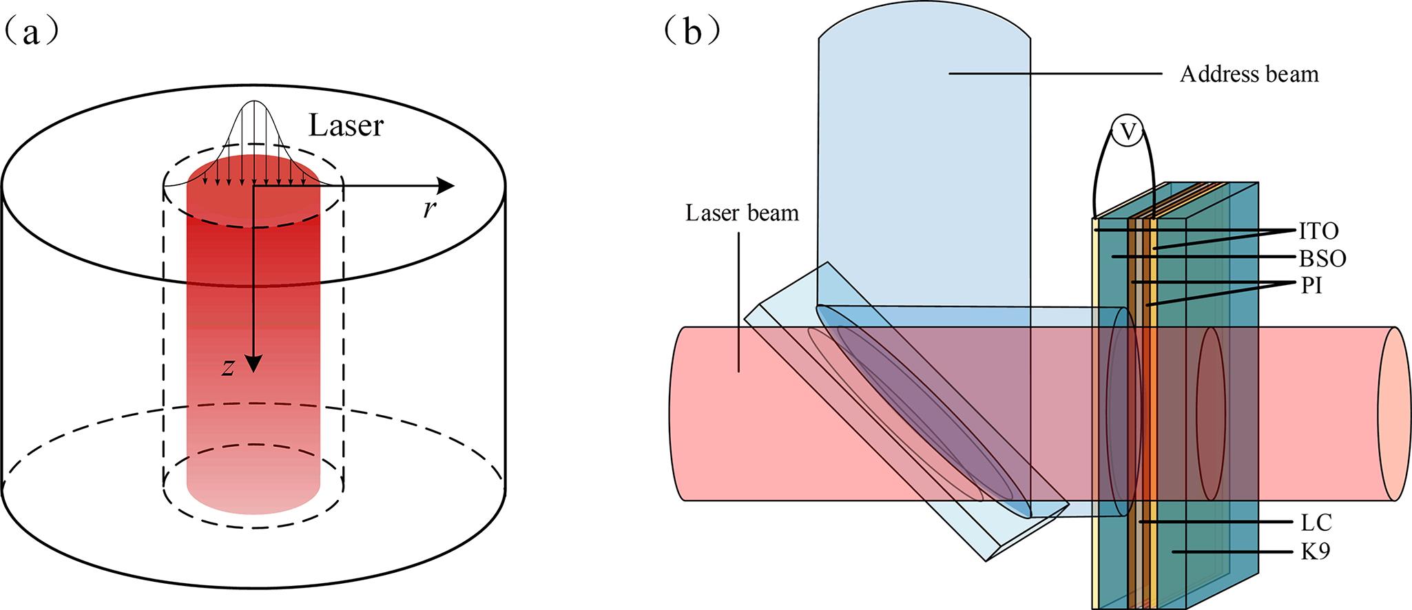
    Fig. 1. (a) Heat transfer equation model. (b) Structure diagram of a laser-irradiated OASLM.
    Simplified heat transfer model.
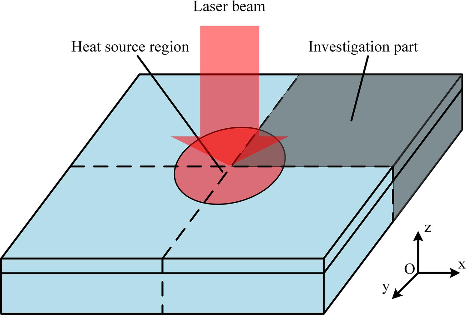
    Fig. 2. Simplified heat transfer model.
    (a) Temperature distribution on the y = 0 plane of a laser-induced liquid crystal light valve. (b) Temperature distribution along the transverse direction of an ITO layer, K9 layer and liquid crystal layer. (c) Temperature distribution along the depth direction at the center of a liquid crystal light valve, the small icon shows the material structure distribution along the Z direction.
    Fig. 3. (a) Temperature distribution on the y = 0 plane of a laser-induced liquid crystal light valve. (b) Temperature distribution along the transverse direction of an ITO layer, K9 layer and liquid crystal layer. (c) Temperature distribution along the depth direction at the center of a liquid crystal light valve, the small icon shows the material structure distribution along the Z direction.
    (a) Relationship between transmittance and temperature of an OASLM. (b) The required adjustment of driving voltage with temperature.
    Fig. 4. (a) Relationship between transmittance and temperature of an OASLM. (b) The required adjustment of driving voltage with temperature.
    Voltage of liquid crystal layer changes with the loaded gray level under different driving conditions.
    Fig. 5. Voltage of liquid crystal layer changes with the loaded gray level under different driving conditions.
    Flow chart of the proposed compensation method.
    Fig. 6. Flow chart of the proposed compensation method.
    Schematic diagram of the OASLM temperature rise performance test experimental system. POL: polarizer, HWP: half wave plate, BS: beam splitter, NDF: neutral density filter, L: lens, and ANA: analyzer.
    Fig. 7. Schematic diagram of the OASLM temperature rise performance test experimental system. POL: polarizer, HWP: half wave plate, BS: beam splitter, NDF: neutral density filter, L: lens, and ANA: analyzer.
    (a) Temperature of the OASLM as a function of laser power density. (b) Transmittance of the OASLM as a function of temperature, where the red data points are the experimental data and the blue curve is the fitting curve.
    Fig. 8. (a) Temperature of the OASLM as a function of laser power density. (b) Transmittance of the OASLM as a function of temperature, where the red data points are the experimental data and the blue curve is the fitting curve.
    (a) Distribution of light field after transmittance and temperature increase at 24 V. (b)–(d) Light field distribution at 22 V, 20 V and 19 V, respectively. (e) OASLM driving voltage as a function of temperature, where red data points represent experimental data. (f) Gamma curves under different driving conditions and different temperatures. Curve 1: 298 K, 24 V, 600 mA; curve 2: 326 K, 24 V, 600 mA; curve 3: 326 K, 19 V, 600 mA; curve 4: 326 K, 19 V, 1000 mA.
    Fig. 9. (a) Distribution of light field after transmittance and temperature increase at 24 V. (b)–(d) Light field distribution at 22 V, 20 V and 19 V, respectively. (e) OASLM driving voltage as a function of temperature, where red data points represent experimental data. (f) Gamma curves under different driving conditions and different temperatures. Curve 1: 298 K, 24 V, 600 mA; curve 2: 326 K, 24 V, 600 mA; curve 3: 326 K, 19 V, 600 mA; curve 4: 326 K, 19 V, 1000 mA.
    (a) Gray level sinusoidal distribution pattern, where the red circle indicates the laser irradiation area. (b) Optical field distribution at 7.5 W/cm2. (c) Optical field distribution at 21 W/cm2. (d) Optical field distribution at 21 W/cm2 after compensation. (e) Comparison of transmittance at section line positions in (b), (c) and (d).
    Fig. 10. (a) Gray level sinusoidal distribution pattern, where the red circle indicates the laser irradiation area. (b) Optical field distribution at 7.5 W/cm2. (c) Optical field distribution at 21 W/cm2. (d) Optical field distribution at 21 W/cm2 after compensation. (e) Comparison of transmittance at section line positions in (b), (c) and (d).
    (a) Binary gray bar pattern, where the red circle indicates the laser irradiation area. (b) Optical field distribution at 7.5 W/cm2. (c) Optical field distribution at 21 W/cm2. (d) Optical field distribution at 21 W/cm2 after compensation. (e) Comparison of transmittance at section line positions in (b), (c) and (d).
    Fig. 11. (a) Binary gray bar pattern, where the red circle indicates the laser irradiation area. (b) Optical field distribution at 7.5 W/cm2. (c) Optical field distribution at 21 W/cm2. (d) Optical field distribution at 21 W/cm2 after compensation. (e) Comparison of transmittance at section line positions in (b), (c) and (d).
    MaterialsK9BSOPIITOLC
    Thermal conductivity (W/mK)1.430.283.30.5
    Absorption coefficient (m–1)0.551×1045×1050.1
    Table 1. Physical parameters of structural materials.
    ParametersValueUnit
    Beam diameter8mm
    Thickness of K93mm
    Thickness of BSO1mm
    Thickness of ITO50nm
    Thickness of ITO100nm
    Thickness of ITO4.8μm
    Table 2. Physical parameters of structural materials.
    Tongyao Du, Dajie Huang, He Cheng, Wei Fan, Zhibo Xing, Xuechun Li, Jianqiang Zhu. Compensation method for performance degradation of optically addressed spatial light modulator induced by CW laser[J]. High Power Laser Science and Engineering, 2022, 10(1): 010000e7
    Download Citation