Abstract
The in-plane anisotropy of transition metal trichalcogenides (MX3) has a significant impact on the molding of materials and MX3 is a perfect choice for polarized photodetectors. In this study, the crystal structure, optical and optoelectronic anisotropy of one kind of quasi-one-dimensional (1D) semiconductors, ZrSe3, are systematically investigated through experiments and theoretical studies. The ZrSe3-based photodetector shows impressive wide spectral response from ultraviolet (UV) to near infrared (NIR) and exhibits great optoelectrical properties with photoresponsivity of 11.9 mA·W-1 and detectivity of ~106 at 532 nm. Moreover, the dichroic ratio of ZrSe3-based polarized photodetector is around 1.1 at 808 nm. This study suggests that ZrSe3 has potential in optoelectronic applications and polarization detectors.The in-plane anisotropy of transition metal trichalcogenides (MX3) has a significant impact on the molding of materials and MX3 is a perfect choice for polarized photodetectors. In this study, the crystal structure, optical and optoelectronic anisotropy of one kind of quasi-one-dimensional (1D) semiconductors, ZrSe3, are systematically investigated through experiments and theoretical studies. The ZrSe3-based photodetector shows impressive wide spectral response from ultraviolet (UV) to near infrared (NIR) and exhibits great optoelectrical properties with photoresponsivity of 11.9 mA·W-1 and detectivity of ~106 at 532 nm. Moreover, the dichroic ratio of ZrSe3-based polarized photodetector is around 1.1 at 808 nm. This study suggests that ZrSe3 has potential in optoelectronic applications and polarization detectors.Introduction
In recent years, transition metal dichalcogenides (TMDCs) have gained attention due to their tunable optical, optoelectrical and physiochemical properties[1] that originate from quantum confinement effects and low dimensionality[2-12]. Meanwhile, layered semiconductor materials and their heterojunctions have potential applications in constructing the next generation of optoelectronic devices[13-16]. As one member in the TMDCs family, transition metal trichalcogenides (MX3) have been a source of attention for many years. The weak van der Waals amalgamated structures of MX3 constitute a distinct family of compounds, where M represents the metal atom from group IV, V or VI and X is chalcogen atom (S, Se or Te)[17-19]. The linear chain of MX3 is parallel to the crystallographicb-axis, six chalcogen atoms surround one metal atom. MX3 bulk materials are wire-like crystals while the counterparts with few layers are nanoribbons with a quasi-1D structure. Previous works have shown that MX3 enjoy strong in-plane optical and electrical anisotropy properties, due to their structural anisotropy[20,21].
Nowadays, most polarization sensitive photodetectors that are composed of an optical medium with polarization effect have realized a high extinction ratio through the polarization selection of plasmon microcavities[22]. However, these polarized photodetectors suffer from several challenges, including complicated fabrication process and high cost. Recently, active materials for polarized photodetector have focused on semiconductors with low symmetry structure[23-25], such as black phosphorus[26], TiS3[20], GeAs[27], GeSe[28]. This work is conducive to the development of polarized photodetectors towards miniaturization and integration. Analogously, quasi-1D ZrSe3 with low-symmetry is an ideal candidate for polarized photodetectors.
In this work, we prepared high-quality ZrSe3 nanowires using the chemical vapor transport (CVT) method. The anisotropic optical and optoelectrical properties of ZrSe3 are confirmed by polarization-resolved optical microscopy (PROM) and polarized optoelectrical measurements. The angularly resolved Raman spectra and polarized light absorption spectroscopy show that ZrSe3 have in-plane anisotropy. Furthermore, the results of the polarized photodetection imply that ZrSe3-based photodetectors are sensitive to linearly polarized light.
Results and discussion
Synthesis and structural analysis
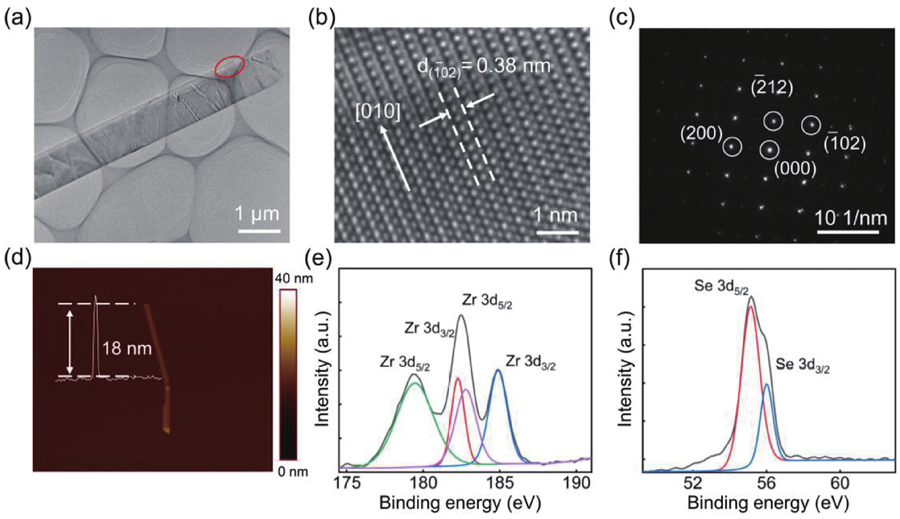
High-quality ZrSe3 nanowires (NWs) were synthesized via the CVT method. Powder Zr (0.45 g) and Se (1.35 g) were mixed in stoichiometric proportions (1 : 3) with 30 mg I2 as transport agent. The sources were then placed in an ampoule that was placed into a double-zone furnace. The temperatures of the high temperature zone and the low temperature zone are set as 650 °C and 500 °C, respectively. The ampoule was heated to 650 °C/500 °C for 24 hours and kept at this temperature for 3 days. After heating, the furnace was cooled to room temperature in 1 day and the ZrSe3 NWs had collected on the inner surface of tube. The structure of ZrSe3 belongs to monoclinic structure witha = 3.788 Å,b = 5.485 Å andc = 10.156 Å, and a symmetry space group of p21/m[29]. Transmission electron microscopy (TEM) is an effective method to characterize crystal microstructure and growth direction.Fig. 1(a) is a low-magnification TEM image of the ZrSe3 NWs. The high-resolution transmission electron microscopy (HRTEM) image (Fig. 1(b)) was obtained from the marked region ofFig. 1(a). As shown inFig. 1(b), the lattice spacing is 0.38 nm, which represents (
) plane, which indicates that the ZrSe3 NWs prefer to grow along theb-axis. The obvious diffraction spots in the selected area electron diffraction (SAED) pattern (Fig. 1(c)) indicate that the ZrSe3 is a single crystal. The diffraction spots agree with (200), (
) and (
) plane, respectively. The elements of Zr and Se are distributed uniformly on the nanowire, as shown in elemental mapping (Fig. S1). The energy-dispersive X-ray spectroscopy (EDX) shows that the elemental stoichiometric ratio is around 1 : 3 (Fig. S2). In addition, the ZrSe3 NWs were measured by atomic force microscopy (AFM) (Fig. 1(d)), which shows that the thicknesses of ZrSe3 are about 18 nm. The chemical state can be characterized through the method of X-ray photoelectron spectroscopy (XPS). As shown inFigs. 1(e) and1(f), the binding energies of 179.48 and 182.78 eV are Zr 3d5/2, 182.28 and 184.88 eV are Zr 3d3/2[30]. This observation is similar with the analysis of HfTe3, in which the Hf was assumed with mixed-valence states[31]. Therefore, we also speculate that Zr4+ (the doublets located at 182.78 and 184.88 eV) and Zr2+ (the doublets located at 179.48 and 182.28 eV) coexist in the ZrSe3 NWs. The peak area shows that the ratio of Zr4+ and Zr2+ is approximately 1 : 1.

Figure 1.(Color online) Characterization of ZrSe3 crystal. (a) Low-magnification transmission electron microscopy (TEM) of the quasi-1D ZrSe3. (b) High-resolution transmission electron microscopy (HRTEM) image of the quasi-1D ZrSe3. (c) Selected area electron diffraction (SAED) pattern of the quasi-1D ZrSe. (d) The AFM image of ZrSe3 crystal. (e) High-resolution spectra of Zr 3d core level. (f) High-resolution spectra of Se 3d core level.
Angle-resolved polarized Raman spectroscopy (ARPRS) is a powerful method to characterize the material structure that can be used to determine the symmetry of chemical bond vibration[32]. The unit cell of ZrSe3 includes eight atoms, giving rise to 24 normal vibration modes. The irreducible representations at the center of Brillouin zone: Г = 8Ag+ 4Bg+ 4Au+ 8Bu. Among these 24 formula units, Ag and Bg modes are Raman active while Au and Bu are infrared-active.Fig. 2(a) shows the Raman spectra of ZrSe3 NWs under 532 nm. It is clear that there are four peaks of normal Raman spectra at or near 107.22, 178.87, 234.61 and 301.4 cm−1, which are all assigned to Ag mode[29]. Furthermore, the polarized Raman spectra was measured in parallel and cross configurations and the ZrSe3 NW was rotated from 0° to 180°. The contour color maps inFig. 2(b) and2(c) show the obvious anisotropy of chemical bond vibration. The typical Raman peaks of 178.9, 234.61 and 301.4 cm–1 are extracted and fitted in polar coordinates (Figs. 2(d) and2(e), Fig. S3). The formula of the fitting curve can be expressed as
[eiRes]2, whereei andes are the polarization vectors of incident light and scattered light, respectively (ei = [cosθ sinθ 0],es// = [cosθ sinθ 0]T,es⊥=[–sinθ cosθ 0]T), andR is the Raman tensor. The Raman tensor of Ag (ZrSe3 correspond to symmetry space group of p21/m) is as follows:
Figure 2.(Color online) (a) Raman spectra under unpolarized and polarized laser (532 nm). (b) Counter maps of angle-resolved Raman spectra under cross configuration. (c) Counter maps of angle-resolved Raman spectra under parallel configuration. (d) Polar plots of angle-resolved and fitted peak intensities of 234.6 cm−1. (e) Polar plots of angle-resolved and fitted peak intensities of 301.4 cm−1.
After calculation, the Raman scattering intensities of Ag mode can be expressed as follows:
The fitting curves of cross configuration show four-leaf shapes. For parallel configuration, the fitting curves show spindle shapes. All of these results indicate that the structure of ZrSe3 crystal is anisotropic.
Theoretical calculations
The schematic crystal structure inFig. 3(a) shows infinite ribbons stacked along theb-axis and the layers are combined with each other through van der Waals interaction. Based on the crystal structure, the theoretical calculation of ZrSe3 is studied. The band structure of ZrSe3 was calculated through Heyd-Scuseria-Ernzerhof hybrid function method (HSE06)[33], exhibiting a band gap of 1.05 eV (Fig. 3(b)). For the theoretical calculation, the generalized gradient approximation PBE (GGA-PBE) of correlation functional and exchange were used in the calculation[34,35]. We then used the hybrid functional (HSE06) method for the accurate calculation of optical property and electronic structure, in which the hybrid functional was mixed with 25% exact Hartree–Fock (HF) exchange[33]. In addition, a Monkhorst-Pack k–mesh of 6 × 9 × 4 sampling in the full Brillouin zone was used in the calculations[36]. The integral path of the band structure is Γ → X → S → Y → Γ. The electronic band structure indicates that the valence band maximum (VBM) is located at the X point and the conduction band minimum (CBM) is located at the Γ point. Moreover, the total density of states (DOS) and partial density of states (PDOS) (Fig. S4(a)) were calculated. It is shown that the top of the valence band is mainly composed of Se’s p orbital of Se atom, while the bottom of the conduction band is mainly made up by Zr’s d orbital of the Zr atom. The dielectric constants along thea-axis andb-axis of ZrSe3 were calculated as shown inFig. 3(c), and the corresponding optical absorbance coefficient (Fig. S4(b)) was calculated theoretically based on the dielectric function[37]. These results show that there is an obvious difference alonga-axis andb-axis from 250 to 820 nm. The electric dipole transition probabilityR is positively related to the electron-radiation interaction |<c|HeR|v>|2, where HeR is Hamiltonian matrix element, |c> and |v> are wave functions of conduction band and valence band[38]. The transition probability (Ra,Rb) from valence band maximum (VBM) to conduction band minimum (CBM) along different k-points path can be calculated throughRa = |<c|HeRa|v>|2/(|<c|HeRa|v>|2 + |<c|HeRb|v>|2),Rb = |<c|HeRb|v>|2/(|<c|HeRa|v>|2 + |<c|HeRb|v>|2). The results ofRa andRb are shown inFig. 3(d). Some typical point, such as S and Y, are selected to be analyzed. For the S point, the probabilityRa is around 0.64 andRb is around 0.36, which means that the strength of absorption alonga-axis is larger than theb-axis. While for the Y point,Ra is very close to 1, which means that around the Y point the absorption only occurred along thea-axis. The difference strengths of absorption along thea-axis andb-axis lead to the polarization sensitive of ZrSe3. Furthermore, the polarization sensitivity of ZrSe3 is influenced by the electron transition of different energy levels and is not limited to the VBM and CBM. This obvious difference of transition probability is based on the charge density distribution alonga andb axes (Figs. 3(e)–3(f)). These results indicate that quasi-1D ZrSe3 enjoys optical and optoelectric anisotropy.
Figure 3.(Color online) (a) Atomic structure of ZrSe3 crystal. (b) Band structure of layered ZrSe3. (c) Calculated real parts and imaginary parts of the dielectric constant alonga-axis andb-axis. (d) TheRa andRb of optical transition |v> → |c> along the k-points path. (e, f) Partial charge density of ZrSe3 at the state of CBM and VBM respectively.
Optical and photoelectrical anisotropy
The optical anisotropy of quasi-1D ZrSe3 was studied through polarization-resolved optical microscopy (PROM). For the PROM test, ZrSe3 NWs were exfoliated on the SiO2/Si substrate, which is isotropic. During the investigation, the direction of polarization analyzer is perpendicular to the linear polarized incident light. It can be seen in Fig. S5 that the images of PROM, which are selected from 0° to 165° by a step of 15° and the brightness of ZrSe3 express obvious light and dark changes. The reason for this phenomenon is that linearly polarized incident light may be refracted into two components with different vibration directions after passing through the birefringent material[39]. The result of PROM indicates that quasi-1D ZrSe3 crystal enjoys obvious anisotropy.
To verify the in-plane optical anisotropy of quasi-1D ZrSe3, we exfoliated and transferred the ZrSe3 crystal onto mica. The measured polarization-resolved absorption spectrum is shown in Fig. S6. It is obvious that the maximum absorption appears in the polarized light of 90°, which corresponds to thea-axis. This happens because the incoming photons more effectively interact with thea-axis[40]. The absorption range covers the entire visible region and part of the near-infrared region, which is nearly coincident with the calculated absorption spectra. To investigate the photoelectric properties of quasi-1D ZrSe3, the few-layers ZrSe3 nanowires with a thickness of 18 nm were exfoliated and transferred onto the SiO2/Si substrate (the thickness of SiO2 is 300 nm). Because the polarized absorption covered from visible to near-infrared range (360–860 nm), some typical wavelengths (360, 450, 532, 638 and 808 nm) were chosen for the photodetection. As shown inFig. 4(a),Figs. 5(a)–5(c) and Fig. S7, the photocurrent increases with the increase of the light power intensity. Specifically, under 532 nm lumination, the photocurrent increases from 127 to 166.5 pA atVds = 5 V with light power intensity from 26.8 to 114.3 mW/cm2 (Fig. 4(a)). The relationship of photocurrent and light power intenstiy can be expressed as:I =αPβ, whereα, β are dimensionless constants and I is photocurrent andP is light power intensity. Under the light irradiation, the photocurrent tends to be saturated with stronger light power intensity, which is related to the fact that carriers could be recombianted under the strong irradiation. The results after fitting are shown inFig. 4(b). Corelatively,β = 0.81, 0.15, 0.16, 0.29 and 0.22 corresponding to 360, 450, 532, 638 and 808 nm, respectively. In addition, the other two parameters of the photodetectors are responsivity (R) and detectivity (D*). Responsivity indicates the ability of photodetectors to convert a light signal into an electrical signal, which can be expressed as:
, where ΔI is the difference of photocurrent and dark current,Pλ is power intensity of incident light andS is the effective area of photodetectors. Detectivity (R*) reflects the sensitivity for perceiving weak light, which can be demonstrated as
, whereR is the responsivity,e is unit charge andId is dark current. As shown inFig. 4(c), the photodetector based on ZrSe3 has good performance in the ultraviolet and near-infrared region, especiallyR andD* reach 11.9 mA/W and around 106 Jones at 532 nm. This happens because the short wavelength laser can excite more electrons that are located at different valence bands to the conduction band. The decrease in the ultraviolet region is due to the increased recombination rate of the carriers. As shown in Fig. S8,I–V curves of ZrSe3-based photodetectors at 360, 450, 638 and 808 nm indicate that the metal-semiconductor contact is an Ohmic contact. Moreover, the rise time is the time from 10% saturated photocurrent to 90% saturated photocurrent and the decay time is the time from 90% saturated photocurrent to 10% saturated photocurrent. The rise time of ZrSe3-based photodetector is around 2.8 s, while for decay time it is about 30 s. The decay time of ZrSe3-based photodetector is longer than the rise time because the surface defect states of ZrSe3 prolong the recombination process of the photogenerated electric-hole pairs. In addition, the short wavelength laser, with larger photon energy, has a higher coupling efficiency leading to thermal heating effect, which results in prolonged response time. The influence of the width of the device is also discussed. The photoelectrical performance of photodetector with different widths (0.7, 1.2, 1.8μm) is measured. The results (Fig. S9) show that the ZrSe3-based photodetector with appropriate width (1.2μm) has better photoelectrical properties.
Figure 4.(Color online) (a) Time-resolved photoresponse of the ZrSe3-based photodetector for a bias voltage of 5 V under 532 nm with different light power density. (b) Dependence of the photocurrent on the intensity of incident laser power. (c) The spectral responsivity and detectivity of ZrSe3-based photodetector. (d) Evolution of the photocurrent with a polarized angle under 532 nm.
Figure 5.(Color online) (a−c) Time-resolved photoresponse of the ZrSe3-based photodetector for a bias voltage of 5 V under 450, 638 and 808 nm with different light power density respectively. (d–f) Evolution of the photocurrent with polarized angles under 450, 638 and 808 nm, respectively.
Raman spectra, PROM and absorption spectra show that ZrSe3 NWs possess an obvious crystal structure and optical anisotropy. These results prompt us to expend the investigation from photoelectric detection to polarized photodetection. The linearly polarized light was obtained through the assistance of Glan-Taylor prism, which acts as a polarizer. In addition, we used the half-wave plate to change the direction of the linearly polarized light. The extinction ratio of polarizer (Glan-Taylor prism) reaches 105 : 1, which guarantees the appearance of the linearly polarized light. The drain–source voltage was fitted at 5 V, the direction of linearly polarized light was rotated with a step of 10° or 20°. The photocurrents with the polarized angle from 0° to 360° were extracted and plotted in polar coordinate system (Fig. 4(d) andFigs. 5 (d) and5(e)). The direction of b-axis of ZrSe3 NWs was defined as 0°. They were then fitted through the equation:
, whereIpha andIphb are the photocurrents alonga-axis andb-axis of ZrSe3 NWs,θ is the polarization angle[41]. The gourd-shaped fitting curves indicate that the ZrSe3-based photodetector enjoys polarization-sensitivity and the largest photocurrents are all reached along thea-axis of ZrSe3 crystal. TheIpha/Iphb ratios at 450, 532, 638 and 808 nm are 1.02, 1.03, 1.02 and 1.1, respectively. The optoelectrical properties of ZrSe3-based photodetector are summarized inTable 1. This shows that the quasi-1D ZrSe3 crystal has application value in the field of optoelectronics.
Table Infomation Is Not Enable
Conclusion
In summary, layered quasi-1D nanowires ZrSe3 were synthesized with the CVT method. The HRTEM, APRPS, PROM, absorption spectroscopy and polarized optoelectronic investigations show the anisotropy of ZrSe3 NWs. The ZrSe3-based photodetector performs a wide photoresponse from UV to NIR with impressive optoelectronic properties, with photoresponsivity of 11.9 mA/W and detectivity of ~106 at 532 nm. It also exhibits polarization-sensitivity due to the anisotropic structure. These results show that quasi-1D ZrSe3 NWs have the potential in application of polarization photodetector without the help of optical polarizer.
Acknowledgements
This work was financially supported by the National Key Research and Development Program of China (Grant No. 2017YFA0207500), the National Natural Science Foundation of China (Grant No. 62125404, 12004375, 62004193, 62174155), the CAS-JSPS Cooperative Research Project (No. GJHZ2021131), and the Strategic Priority Research Program of Chinese Academy of Sciences (Grant No. XDB43000000).
Appendix A. Supplementary materials
Supplementary materials to this article can be found online athttps://doi.org/10.1088/1674-4926/43/10/102001.
References
[1] B Radisavljevic, A Radenovic, J Brivio et al. Single-layer MoS2 transistors. Nat Nanotechnol, 6, 147(2011).
[2] A Patra, C S Rout. Anisotropic quasi-one-dimensional layered transition-metal trichalcogenides: Synthesis, properties and applications. RSC Adv, 10, 36413(2020).
[3] Q N Cui, A Lipatov, J S Wilt et al. Time-resolved measurements of photocarrier dynamics in TiS3 nanoribbons. ACS Appl Mater Interfaces, 8, 18334(2016).
[4] I J Ferrer, J R Ares, J M Clamagirand et al. Optical properties of titanium trisulphide (TiS3) thin films. Thin Solid Films, 535, 398(2013).
[5] I J Ferrer, M D Maciá, V Carcelén et al. On the photoelectrochemical properties of TiS3 films. Energy Procedia, 22, 48(2012).
[6] S J Gilbert, A Lipatov, A J Yost et al. The electronic properties of Au and Pt metal contacts on quasi-one-dimensional layered TiS3(001). Appl Phys Lett, 114, 101604(2019).
[7] J O Island, M Buscema, M Barawi et al. Ultrahigh photoresponse of few-layer TiS3 nanoribbon transistors. Adv Opt Mater, 2, 641(2014).
[8] N Papadopoulos, R Frisenda, R Biele et al. Large birefringence and linear dichroism in TiS3 nanosheets. Nanoscale, 10, 12424(2018).
[9] A Pant, E Torun, B Chen et al. Strong dichroic emission in the pseudo one dimensional material ZrS3. Nanoscale, 8, 16259(2016).
[10] Y Xiao, M Y Zhou, J L Liu et al. Phase engineering of two-dimensional transition metal dichalcogenides. Sci China Mater, 62, 759(2019).
[11] H Huang, M Gao, J H Wang et al. Intercalator-assisted plasma-liquid technology: An efficient exfoliation method for few-layer two-dimensional materials. Sci China Mater, 63, 2079(2020).
[12] Y L Huang, W Chen, A T S Wee. Two-dimensional magnetic transition metal chalcogenides. SmartMat, 2, 139(2021).
[13] Z C Zhang, B Zhao, D Y Shen et al. Synthesis of ultrathin 2D nonlayered α-MnSe nanosheets, MnSe/WS2 heterojunction for high-performance photodetectors. Small Struct, 2, 2100028(2021).
[14] X Han, Z S Xu, W Q Wu et al. Recent progress in optoelectronic synapses for artificial visual-perception system. Small Struct, 1, 2000029(2020).
[15] X Y Tian, Y S Liu. Van der Waals heterojunction ReSe2/WSe2 polarization-resolved photodetector. J Semicond, 42, 032001(2021).
[16] H H Fang, W D Hu. Hybrid heterojunctions based on 2D materials and 3D thin-films for high-performance photodetectors. Sci China Phys Mech Astron, 60, 027031(2017).
[17] F Iyikanat, R T Senger, F M Peeters et al. Quantum-transport characteristics of a p-n junction on single-layer TiS3. Chemphyschem, 17, 3985(2016).
[18] R Sun, Y Gu, G F Yang et al. Theoretical study on the interfacial properties of monolayer TiS3-metal contacts for electronic device applications. J Phys Chem C, 123, 7390(2019).
[19] J Kang, L W Wang. Robust band gap of TiS3 nanofilms. Phys Chem Chem Phys, 18, 14805(2016).
[20] S J Liu, W B Xiao, M Z Zhong et al. Highly polarization sensitive photodetectors based on quasi-1D titanium trisulfide (TiS3). Nanotechnology, 29, 184002(2018).
[21] X T Wang, K D Wu, M Blei et al. Highly polarized photoelectrical response in vdW ZrS3 nanoribbons. Adv Electron Mater, 5, 1900419(2019).
[22] L Li, D Y Xiong, J Wen et al. A surface plasmonic coupled mid-long-infrared two-color quantum cascade detector. Infrared Phys Technol, 79, 45(2016).
[23] J Gao, Y Zheng, W Yu et al. Intrinsic polarization coupling in 2D α-In2Se3 toward artificial synapse with multimode operations. SmartMat, 2, 88(2021).
[24] Z Q Zhou, Y Cui, P H Tan et al. Optical and electrical properties of two-dimensional anisotropic materials. J Semicond, 40, 061001(2019).
[25] J Z Fang, Z Q Zhou, M Q Xiao et al. Recent advances in low-dimensional semiconductor nanomaterials and their applications in high-performance photodetectors. InfoMat, 2, 291(2020).
[26] M S Long, A Y Gao, P Wang et al. Room temperature high-detectivity mid-infrared photodetectors based on black arsenic phosphorus. Sci Adv, 3, e1700589(2017).
[27] Z Q Zhou, M S Long, L F Pan et al. Perpendicular optical reversal of the linear dichroism and polarized photodetection in 2D GeAs. ACS Nano, 12, 12416(2018).
[28] X T Wang, Y T Li, L Huang et al. Short-wave near-infrared linear dichroism of two-dimensional germanium selenide. J Am Chem Soc, 139, 14976(2017).
[29] K Osada, S Bae, M Tanaka et al. Phonon properties of few-layer crystals of quasi-one-dimensional ZrS3 and ZrSe3. J Phys Chem C, 120, 4653(2016).
[30] X Yu, X K Wen, W F Zhang et al. Fast and controlled growth of two-dimensional layered ZrTe3 nanoribbons by chemical vapor deposition. CrystEngComm, 21, 5586(2019).
[31] J Li, J Peng, S Zhang et al. Anisotropic multichain nature and filamentary superconductivity in the charge density wave system HfTe3. Phys Rev B, 96, 174510(2017).
[32] J X Wu, N N Mao, L M Xie et al. Identifying the crystalline orientation of black phosphorus using angle-resolved polarized Raman spectroscopy. Angew Chem Int Ed, 54, 2366(2015).
[33] J Heyd, G E Scuseria, M Ernzerhof. Hybrid functionals based on a screened Coulomb potential. J Chem Phys, 118, 8207(2003).
[34] J P Perdew, K Burke, Y Wang. Generalized gradient approximation for the exchange-correlation hole of a many-electron system. Phys Rev B, 54, 16533(1996).
[35] J P Perdew, K Burke, M Ernzerhof. Generalized gradient approximation made simple. Phys Rev Lett, 77, 3865(1996).
[36] H J Monkhorst, J D Pack. Special points for Brillouin-zone integrations. Phys Rev B, 13, 5188(1976).
[37] S Saha, T P Sinha, A Mookerjee. Electronic structure, chemical bonding, and optical properties of paraelectric BaTiO3. Phys Rev B, 62, 8828(2000).
[38] K Zhao, J H Yang, M Z Zhong et al. Direct polarimetric image sensor and wide spectral response based on quasi-1D Sb2S3 nanowire. Adv Funct Mater, 31, 2006601(2021).
[39] S J Hou, Z F Guo, J H Yang et al. Birefringence and dichroism in quasi-1D transition metal trichalcogenides: Direct experimental investigation. Small, 17, e2100457(2021).
[40] H Yang, L F Pan, X T Wang et al. Mixed-valence-driven quasi-1D SnIISnIVS3 with highly polarization-sensitive UV-vis-NIR photoresponse. Adv Funct Mater, 29, 1904416(2019).
[41] M Q Xiao, H Yang, W F Shen et al. Polarization-sensitive photodetectors: Symmetry-reduction enhanced polarization-sensitive photodetection in core-shell SbI3/Sb2O3 van der Waals heterostructure. Small, 16, 2070036(2020).