
Kejian Zhu, Pengfei Sun, Pengfei Xu, Xingpeng Liu, Tangyou Sun, Haiou Li, Zhiping Zhou. Kerr effect in ultra-compact hybrid plasmonic metal-insulator-metal nano-focusing structure[J]. Chinese Optics Letters, 2022, 20(3): 031903
- Chinese Optics Letters
- Vol. 20, Issue 3, 031903 (2022)
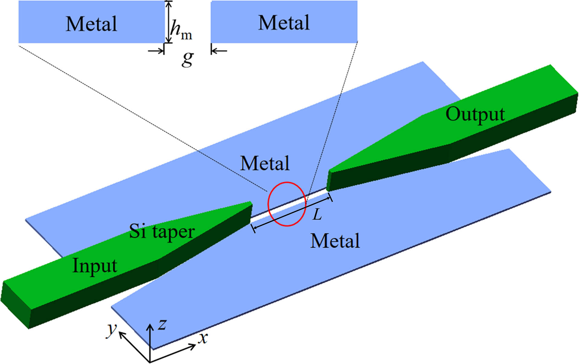
Fig. 1. Schematic of the proposed MIM 2D HPWG nano-focusing structure, which is usually based on the SOI substrate. The tip width of the Si taper is wtip, which is from zero to the width of the dielectric waveguide.
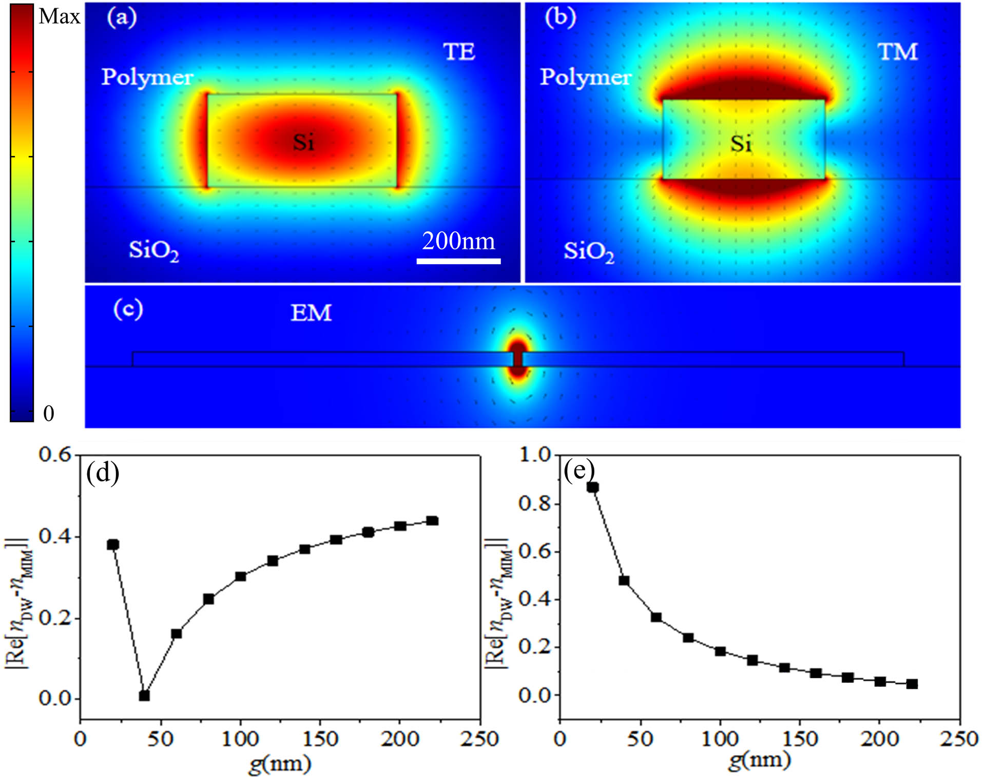
Fig. 2. Eigenmode (a) TE and (b) TM electric field distribution diagrams of the dielectric waveguide, (c) eigenmode EM electric field distribution diagram of the MIM waveguide. (d) The absolute value of the difference between the real part of the effective refractive index of the EM and the real part of the effective refractive index of the dielectric waveguide TE. (e) The absolute value of the difference between the real part of the effective refractive index of the EM and the real part of the effective refractive index of the dielectric waveguide TM. λ = 1550 nm.
Fig. 3. Relationship between the real part of the effective refractive index of EM and MIM metal layer gap g based on SOI for λ = 1550 nm.
Fig. 4. (a) Field distribution of the MIM nano-focusing structure when the TE mode is incident. Along the x direction, (b) x1 = −2.5 µm, (c) x2 = −1.8 µm, (d) x3 = −1 µm, and (e) x4 = 0 µm on cross-section electric field component contour map, where the weight in the lower right corner of each figure represents the size of the voltage value range of the contour map. The larger the weight, the larger the voltage range used when drawing. (f) The absolute value of the maximum electric field corresponding to different positions of x; the electric field value in the focus area is obviously larger, indicating that the focusing effect is significant. (g) The gap width g dependence of insertion loss. λ = 1550 nm, hm = 20 nm, wtip = 0, g = 20 nm.
Fig. 5. Effective area Aeff of the MIM nano-focusing structure versus x based on the SOI substrate, for which λ = 1550 nm, hm = 20 nm, wtip = 0, g = 20 nm.
Fig. 6. Change rate of nonlinear phase shift Δϕ of the MIM nano-focusing structure versus x based on the SOI substrate, for which λ = 1550 nm, hm = 20 nm, wtip = 0, g = 20 nm.

Set citation alerts for the article
Please enter your email address
© Copyright 2018-2021 | Chinese Laser Press. All Rights Reserved 沪ICP备15018463号-20