
Kejian Zhu, Pengfei Sun, Pengfei Xu, Xingpeng Liu, Tangyou Sun, Haiou Li, Zhiping Zhou. Kerr effect in ultra-compact hybrid plasmonic metal-insulator-metal nano-focusing structure[J]. Chinese Optics Letters, 2022, 20(3): 031903
- Chinese Optics Letters
- Vol. 20, Issue 3, 031903 (2022)
Abstract
1. Introduction
With the advent of the era of big data, the transmission and processing of massive data puts forward higher requirements on communication systems[
The Kerr effect is the quadratic electro-optic effect, which is the change in the refractive index of a material in response to an external electric field. The Kerr effect has already enabled a range of capabilities, such as signal switching, de-multiplexing, wavelength conversion, light amplification, and supercontinuum generation[
The most commonly used microelectronics integration platform is silicon-on-insulator (SOI). Silicon’s high refractive index and large third-order susceptibility enable efficient nonlinear interactions at relatively low power levels in SOI waveguides approximately 5 cm in length[
Sign up for Chinese Optics Letters TOC. Get the latest issue of Chinese Optics Letters delivered right to you!Sign up now
Two alternative platforms that may be added to the backend stage of a CMOS fabrication process have been proposed and demonstrated to enhance the effective nonlinearity. The first of these, a polymer-silicon platform, combines SOI waveguides with specially designed polymers to increase nonlinear effects, as has been shown with a silicon slot waveguide filled with the nonlinear polymer 2-[4-(dimethylamino)phenyl]-3-{[4-(dimethylamino)phenyl]ethynyl}buta-1,3-diene-1,1,4,4-tetracarbonitrile (DDMEBT)[
Typical surface plasmon waveguide architectures include insulator-metal-insulator (IMI)[
Strong confining MIM waveguides require a full vectorial model for a rigorous description of the nonlinear parameter , which quantifies the strength of the nonlinear effect[
This article aims to study the Kerr effect within typical highly efficient MIM nano-focusing structures by analyzing the material and mode properties that contribute to the nonlinear parameter. In addition, we analyze the third-order nonlinear parameter of the MIM nano-focusing structure and its dependence on the different key structural contributions, both with and without the nonlinear materials.
2. Structure and Principle
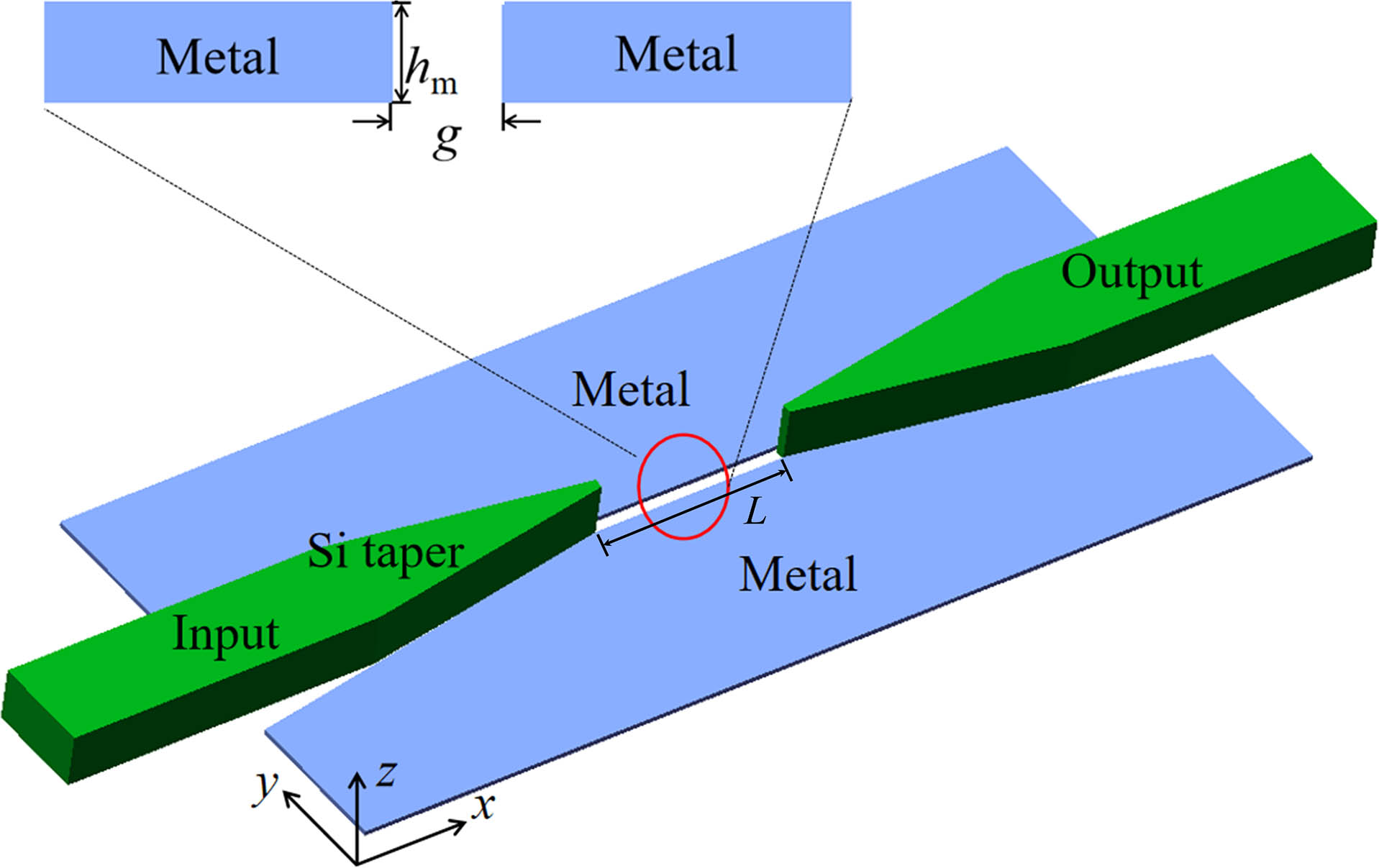
Figure 1 shows the MIM plasmonic nano-focusing structure geometry, for which five regions of different materials are identified: substrate ( with refractive index ), cladding (polymer with refractive index ), dielectric waveguide (Si with refractive index ), metallic waveguide (Au with refractive index ), and spacer (the same as the cladding material). The length of the middle slot waveguide is 0.8 µm.
![]()
Figure 1.Schematic of the proposed MIM 2D HPWG nano-focusing structure, which is usually based on the SOI substrate. The tip width of the Si taper is wtip, which is from zero to the width of the dielectric waveguide.
3. Device Analysis
The nonlinear parameter and effective area can be expressed as follows[
So, a mode strongly compressed by the MIM within a highly nonlinear polymer material has a large effective nonlinear refractive index.
We use the finite element method (COMSOL Multiphysics) to calculate the eigenmodes of the dielectric waveguide and MIM waveguide, respectively, as shown in Fig. 2. To achieve a higher focusing factor, it is necessary to design the structure of the MIM in order to make the effective refractive index difference between the eigenmode (EM) and the dielectric waveguide TE as small as possible and the effective refractive index difference between the eigenmode EM and the dielectric waveguide TM as large as possible. As shown in Figs. 2(d) and 2(e), when nm, the real part of the effective refractive index difference between EM and TE is less than 0.4. In the range of nm, the real part of the effective refractive index difference between EM and TM is greater than 0.3. Therefore, to convert light energy into EM as much as possible, the value of should be less than 60 nm. It should be noted that the focusing effect of EM is also related to factors such as mode similarity and effective area, so the optimal focusing structure should be selected in combination with other key parameters. In this paper, we mainly study the focusing principles of MIM and its corresponding nonlinear analysis.
![]()
Figure 2.Eigenmode (a) TE and (b) TM electric field distribution diagrams of the dielectric waveguide, (c) eigenmode EM electric field distribution diagram of the MIM waveguide. (d) The absolute value of the difference between the real part of the effective refractive index of the EM and the real part of the effective refractive index of the dielectric waveguide TE. (e) The absolute value of the difference between the real part of the effective refractive index of the EM and the real part of the effective refractive index of the dielectric waveguide TM. λ = 1550 nm.
It is found that when the TE mode is incident, the metal can limit the light field near its MIM gap, forming the mixed TE mode (EM1). The mixed TE mode is very different from the TE mode in ordinary media, and it will form obvious reflection on the interface of the metal region and the medium region. On the other hand, the light confinement of metal makes the effective refractive index of the EM1 mode significantly increase, while EM2 and EM3 change very slowly with . These characteristics result in forming a reflective MIM structure, as shown in Fig. 3.
![]()
Figure 3.Relationship between the real part of the effective refractive index of EM and MIM metal layer gap g based on SOI for λ = 1550 nm.
Figure 4 shows the field distribution of the MIM nano-focusing structure with TE mode input. According to the research of Zhu et al., the continuity of the structure generally contributes to the increase of the device bandwidth. In the mode conversion region, the eigenmodes of the silicon wavguide gradually transform to the eigenmodes of the MIM plasmonic waveguide. The gap width and the lateral size of the silicon waveguide affect the eigenmodes of silicon and MIM plasmonic waveguide, which influence the hybrid mode in the conversion region. The difference of electric field polarization before and after the conversion region leads to the increase of reflection rate and insertion loss[
![]()
Figure 4.(a) Field distribution of the MIM nano-focusing structure when the TE mode is incident. Along the x direction, (b) x1 = −2.5 µm, (c) x2 = −1.8 µm, (d) x3 = −1 µm, and (e) x4 = 0 µm on cross-section electric field component contour map, where the weight in the lower right corner of each figure represents the size of the voltage value range of the contour map. The larger the weight, the larger the voltage range used when drawing. (f) The absolute value of the maximum electric field corresponding to different positions of x; the electric field value in the focus area is obviously larger, indicating that the focusing effect is significant. (g) The gap width g dependence of insertion loss. λ = 1550 nm, hm = 20 nm, wtip = 0, g = 20 nm.
Figure 5 shows as a function of positions. It can be seen that in the range of the MIM mode, it is noted that the smaller the gap between metals, the smaller the , but the first decreases as decreases. The size of the effective area directly determines the focusing ability of the nano-focusing device and other characteristics, thereby determining the strength of the Kerr nonlinearity of the nano-focusing device. It can be seen from Eq. (1) that under the premise that the average value of is as large as possible, the smaller the , the more favorable it is to obtain a larger Kerr nonlinear parameter.
![]()
Figure 5.Effective area Aeff of the MIM nano-focusing structure versus x based on the SOI substrate, for which λ = 1550 nm, hm = 20 nm, wtip = 0, g = 20 nm.
Next, we study the magnitude of the nonlinear phase shift of the MIM. The length of the nano-focusing area of this MIM , the linear loss coefficient , and the input power is , so the phase shift can be expressed as[
Figure 6 shows the change rate of nonlinear phase shift as a function of . So, in terms of alone, the position where the nonlinear Kerr effect is around the strongest should be the position near , not the MIM center position. The Kerr nonlinear phase shift corresponding to this position is about 4. Of course, the specific optimal value needs to be determined in combination with other focusing parameters. According to above analysis with at the center of the MIM at 20 nm, there is still improvement space for this value. It is noted that the position with the best MIM focusing effect is absolutely consistent with the area with the greatest nonlinear effect, indicating that the final focusing effect can be obtained after all the structural parameters and other factors are taken into consideration.
![]()
Figure 6.Change rate of nonlinear phase shift Δϕ of the MIM nano-focusing structure versus x based on the SOI substrate, for which λ = 1550 nm, hm = 20 nm, wtip = 0, g = 20 nm.
4. Conclusion
In this paper, we analyze in detail the focusing performance of the MIM nano-focusing device and the strength of the corresponding nonlinear effect when the MIM gap material is a polymer material. The nonlinear effective area and phase shift under different light intensities in different focus areas are quantitatively calculated. After comprehensively considering all factors, it is finally found that the nonlinear effect is the strongest not in the center but in the left side of the MIM structure. We show that the hybrid MIM nano-focusing device is suitable for generating large phase shifts in short propagation length. With larger nonlinear parameters and acceptable propagation loss, the hybrid MIM nano-focusing devices can accumulate a nonlinear phase shift faster than conventional silicon waveguides. By further optimizing the structure and applying materials with larger nonlinear coefficients, these advantages of a hybrid MIM nano-focusing device will play a key role in reducing the footprint of nonlinear optical devices. From this result, we can achieve stronger Kerr nonlinear effects with specific application scenarios.
References
[1] Z. Zhou, R. Chen, X. Li, T. Li. Development trends in silicon photonics for data centers. Opt. Fiber Technol., 44, 13(2018).
[2] Z. Zhou, B. Yin, Q. Deng, X. Li, J. Cui. Lowering the energy consumption in silicon photonic devices and systems [Invited]. Photonics Res., 3, B28(2015).
[3] Z. Zhou, B. Yin, J. Michel. On-chip light sources for silicon photonics. Light Sci. Appl., 4, e358(2015).
[4] F. J. Diaz, G. Li, C. M. de Sterke, B. T. Kuhlmey, S. Palomba. Kerr effect in hybrid plasmonic waveguides. J. Opt. Soc. Am. B, 33, 957(2016).
[5] J. Leuthold, C. Koos, W. Freude. Nonlinear silicon photonics. Nat. Photonics, 4, 535(2010).
[6] D. Dai, J. E. Bowers. Silicon-based on-chip multiplexing technologies and devices for peta-bit optical interconnects. Nanophotonics, 3, 283(2014).
[7] D. Dai, J. Bauters, J. E. Bowers. Passive technologies for future large-scale photonic integrated circuits on silicon: polarization handling, light non-reciprocity and loss reduction. Light Sci. Appl., 1, e1(2012).
[8] Q. Lin, O. J. Painter, G. P. Agrawal. Nonlinear optical phenomena in silicon waveguides: modeling and applications. Opt. Express, 15, 16604(2007).
[9] Z. Zhou, Z. Tu, B. Yin, W. Tan, L. Yu, H. Yi, X. Wang. Development trends in silicon photonics. Chin. Opt. Lett., 11, 012501(2013).
[10] Beyond the diffraction limit. Nat. Photonics, 3, 361(2009).
[11] C. Koos, P. Vorreau, T. Vallaitis, P. Dumon, W. Bogaerts, R. Baets, B. Esembeson, I. Biaggio, T. Michinobu, F. Diederich, W. Freude, J. Leuthold. All-optical high-speed signal processing with silicon–organic hybrid slot waveguides. Nat. Photonics, 3, 216(2009).
[12] B. Esembeson, M. L. Scimeca, T. Michinobu, F. Diederich, I. Biaggio. A high-optical quality supramolecular assembly for third-order integrated nonlinear optics. Adv. Mater., 20, 4584(2008).
[13] D. Dai, S. He. A silicon-based hybrid plasmonic waveguide with a metal cap for a nano-scale light confinement. Opt. Express, 17, 16646(2009).
[14] R. F. Oulton, V. J. Sorger, D. A. Genov, D. F. P. Pile, X. Zhang. A hybrid plasmonic waveguide for subwavelength confinement and long-range propagation. Nat. Photonics, 2, 496(2008).
[15] Z. Zhou, B. Bai, L. Liu. Silicon on-chip PDM and WDM technologies via plasmonics and subwavelength grating. IEEE J. Sel. Top. Quantum Electron., 25, 4600413(2019).
[16] K. Zhu, P. Xu, P. Sun, X. Liu, H. Li, Z. Zhou. An ultra-compact broadband TE-pass nanofocusing structure. Asia Communications and Photonics Conference/International Conference on Information Photonics and Optical Communications, M4A.151(2020).
[17] K. Zhu, P. Xu, P. Sun, X. Liu, H. Li, Z. Zhou. Low loss, high extinction ratio plasmonic spot size converter. Asia Communications and Photonics Conference/International Conference on Information Photonics and Optical Communications, M4A.31(2020).
[18] F. J. Diaz, T. Hatakeyama, J. Rho, Y. Wang, K. O. Brien, X. Zhang, C. Martijn De Sterke, B. T. Kuhlmey, S. Palomba. Sensitive method for measuring third order nonlinearities in compact dielectric and hybrid plasmonic waveguides. Opt. Express, 24, 545(2016).
[19] M. Spasenović, A. Polman, L. K. Kuipers, E. Verhagen. Nanowire plasmon excitation by adiabatic mode transformation. Phys. Rev. Lett., 102, 203904(2009).
[20] J. A. Dionne, H. J. Lezec, H. A. Atwater. Highly confined photon transport in subwavelength metallic slot waveguides. Nano Lett., 6, 1928(2006).
[21] B. Steinberger, A. Hohenau, H. Ditlbacher, A. L. Stepanov, A. Drezet, F. R. Aussenegg, A. Leitner, J. R. Krenn. Dielectric stripes on gold as surface plasmon waveguides. Appl. Phys. Lett., 88, 094104(2006).
[22] K.-Y. Jung, F. L. Teixeira, R. M. Reano. Surface plasmon coplanar waveguides: mode characteristics and mode conversion losses. IEEE Photonics Technol. Lett., 21, 630(2009).
[23] S. I. Bozhevolnyi, V. S. Volkov, E. Devaux, J. Laluet, T. W. Ebbesen. Channel plasmon subwavelength waveguide components including interferometers and ring resonators. Nature, 440, 508(2006).
[24] D. F. P. Pile, T. Ogawa, D. K. Gramotnev, T. Okamoto, M. Haraguchi, M. Fukui, S. Matsuo. Theoretical and experimental investigation of strongly localized plasmons on triangular metal wedges for subwavelength waveguiding. Appl. Phys. Lett., 87, 061106(2005).
[25] Y. Bian, Q. Gong. Low-loss light transport at the subwavelength scale in silicon nano-slot based symmetric hybrid plasmonic waveguiding schemes. Opt. Express, 21, 23907(2013).
[26] K. Adhem, I. Avrutsky. Local field enhancement on demand based on hybrid plasmonic-dielectric directional coupler. Opt. Express, 24, 5699(2016).
[27] M. Z. Alam, J. Stewart Aitchison, M. Mojahedi. Theoretical analysis of hybrid plasmonic waveguide. IEEE J. Sel. Top. Quantum Electron., 19, 4602008(2013).
[28] V. Shahraam Afshar, T. M. Monro. A full vectorial model for pulse propagation in emerging waveguides with subwavelength structures part I: Kerr nonlinearity. Opt. Express, 17, 2298(2009).
[29] A. Pitilakis, E. E. Kriezis. Highly nonlinear hybrid silicon-plasmonic waveguides: analysis and optimization. J. Opt. Soc. Am. B, 30, 1954(2013).
[30] V. Shahraam Afshar, T. M. Monro, C. M. de Sterke. Understanding the contribution of mode area and slow light to the effective Kerr nonlinearity of waveguides. Opt. Express, 21, 18558(2013).
[31] G. Li, C. M. de Sterke, S. Palomba. Figure of merit for Kerr nonlinear plasmonic waveguides. Laser Photonics Rev., 10, 639(2016).
[32] R. Chen, B. Bai, F. Yang, Z. Zhou. Ultra-compact hybrid plasmonic mode convertor based on unidirectional eigenmode expansion. Opt. Lett., 45, 803(2020).
[33] G. P. Agrawal. Nonlinear Fiber Optics(2000).

Set citation alerts for the article
Please enter your email address
© Copyright 2018-2021 | Chinese Laser Press. All Rights Reserved 沪ICP备15018463号-20