
Yue Li, Ming Gong, Hualing Zeng. Atomically thin α-In2Se3: an emergent two-dimensional room temperature ferroelectric semiconductor[J]. Journal of Semiconductors, 2019, 40(6): 061002
- Journal of Semiconductors
- Vol. 40, Issue 6, 061002 (2019)
Abstract
1. Introduction
Owning the switchable and non-volatile electric polarizations at room temperature, conventional ferroelectrics, such as complex perovskite oxides, have broad applications in electronics, including high energy density capacitor[
In the early days of the research on vdW materials, 2D ferroelectricity is lack of attention with rare findings. The reason is that when the thickness is reduced to nanometer scale, the competition between crystal structure stability and the long-range ordering of electric dipoles will become significant. Thus, for a long time, it is hard to get stable crystal phase with switchable electric polarizations in vdW materials under ambient conditions. As ferroelectrics, the prerequisite is the inversion symmetry breaking in structure. For most of the commonly studied 2D materials, taking graphene as a typical example[
The 2D nature of vdW materials allows to explore ferroelectricity in both the in-plane and out-of-plane directions. The in-plane vdW ferroelectrics provide a platform to study domain physics at 2D limit, while the out-of-plane ferroelectric polarizations lay down the fundamental for device applications. In recent years, several candidates of 2D ferroelectrics have been theoretically predicated and verified experimentally. The first example is the layered CuInP2S6. In 2015, Belianinov et al.[
In view of the rapid growing research interest in the 2D ferroelectricity of α-In2Se3, we review some recent relevant progresses in this article. We begin with the introduction of the crystal structure of α-In2Se3 and the corresponding ferroelectricity. The experimental verifications of the in-plane and out-of-plane electric polarizations in ultra-thin α-In2Se3 will be highlighted. Finally, we present two prototypes of ferroelectric devices to demonstrate the potential device application of 2D ferroelectric α-In2Se3.
2. Crystal structure of layered α-In2Se3
Layered In2Se3 is an available 2D semiconductor with remarkable optical and electrical properties[
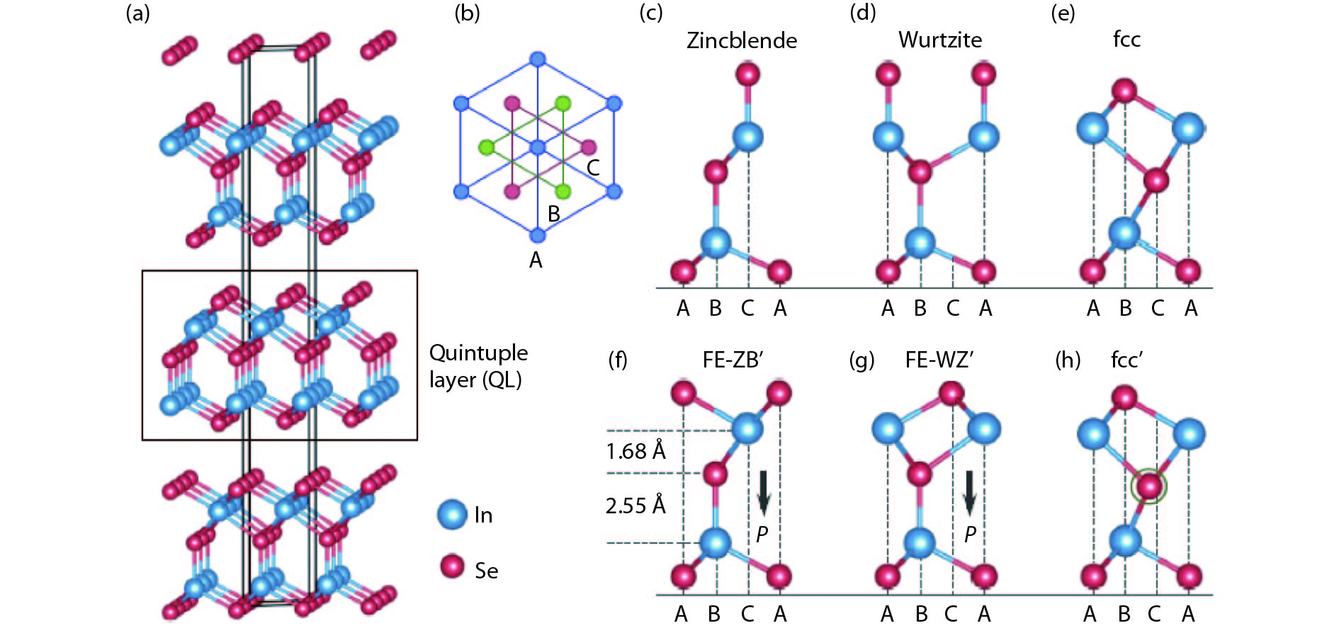
![]()
Figure 1.(Color online) Layered structures of In2Se3. (a) Three-dimensional crystal structure of layered In2Se3, with the In atoms in blue and Se atoms in red, and a quintuple layer (QL) is indicated by the black dashed square. (b) Top view of the system along the vertical direction. Each atomic layer in a QL contains only one elemental species, with the atoms arranged in one of the triangular lattices A, B or C as illustrated. (c–h) Side views of several representative structures of one QL In2Se3, among which the (c) to (e) structures are derived from the zincblende, wurtzite and fcc crystals, respectively. In (f), the interlayer spacings between the central Se layer and the two neighboring In layers are displayed. The black arrows in (f) and (g) indicate the directions of the spontaneous electric polarization (P) in the FE-ZB' and FE-WZ' structures, respectively. The FE-ZB’ and FE-WZ’ structures in (f) and (g) are identified as
To clarify the crystal structure of In2Se3, Ding et al.[
As for ferroelectrics, one important signature is the switchable electric polarization with external stimulus such as electric field. For α-In2Se3, intuitively, the degenerate polarization states with opposite polarity can be achieved by in-plane 180° rotation of a single QL without changing the crystal structure and symmetry. It has been theoretically suggested that the transformation of these two polarization states is kinetically feasible[
3. Experimental verification of coupled ferroelectricity in 2D α-In2Se3
Inspired by the previous theoretical prediction, several groups have aimed to experimentally verify the room temperature ferroelectricity in α-phase In2Se3[
![]()
Figure 2.(Color online) Ferroelectricity of
Another method to study the 2D ferroelectricity in vdW materials is the optical SHG technique, which is a direct probe of the lattice inversion symmetry breaking. With this technique, Xiao et al.[
![]()
Figure 3.(Color online) Electrically switching the out-of-plane ferroelectric polarization and corresponding in-plane atomic configuration through dipole locking. (a) The hysteresis of remnant out-of-plane polarization of a 3-nm-thick In2Se3 crystal on conductive SrRuO3, as a function of perpendicular poling voltage. Black, red, blue curves represent the normalized piezoresponse measured with
4. Ferroelectric device application of atomically thin α-In2Se3
The vacuum potential difference between the top and bottom surfaces of a given α-In2Se3 QL can be as high as 1.4 eV[
We firstly introduce the ferroelectric diode application based on 2D α-In2Se3. With the out-of-plane ferroelectricity of α-In2Se3, a polarity switchable ferroelectric diode with the vertical few-layer graphene/α-In2Se3/graphene heterojunction is proposed and experimentally demonstrated[
![]()
Figure 4.(Color online) Switchable ferroelectric diode based on
A second typical example of the ferroelectric device application is the nonvolatile memory via the device so called FeFET, which is a kind of the three-terminal device by separating the reading operation in the conducting channel from the writing operation in and the ferroelectric gate. FeFETs are non-destructive with no requirement on ferroelectric film thickness. However, the thickness of ferroelectric used in conventional FeFET devices are usually of several hundred nanometers due to the constraint of Critical size effect. Therefore, relatively large operation gate voltage is always required. In contrast, 2D ferroelectrics will significantly scale down the dimensions of the device and meanwhile the voltage to flip the electric polarization could be lowered down dramatically, resulting a low-power consumption memory device.
Fig. 5 shows the schematic and optical image of a FeFET device based on graphene and ferroelectric α-In2Se3[
![]()
Figure 5.(Color online) Structure and optical characterization of the 2D FeFET. (a) 3D schematic diagram of the FeFET. The FeFET is fabricated by vertically stacking graphene, hBN, and
5. Conclusions and outlooks
The vdW materials are promising for realizing 2D ferroelectricity which is the long-sought goal in conventional ferroelectrics. Recent progresses, especially the studies on ultra-thin ferroelectric α-In2Se3, have confirmed their practicability in device applications. They offer a versatile platform to study the ferroelectricity, domain physics, and ferroelectric device at nanometer scale. For α-In2Se3, due to its unique lattice structure, the in-plane and out-of-plane polarizations are inherently coupled, which provides a novel opportunity to control the out-of-plane ferroelectricity by in-plane electric field. However, one of the major bottlenecks for developing 2D ferroelectrics lies in the imperfect sample quality and uniformity. Large-scale ferroelectric thin-film synthesis techniques, such as molecular beam epitaxy (MBE) and chemical vapor deposition (CVD), are highly desired for future practical device application.
Acknowledgments
This work was supported by the National Key Research and Development Program of China (Grant Nos. 2017YFA0205004, 2018YFA03066004, and 2016YFA0301700), the National Natural Science Foundation of China (Grant Nos. 11674295 and 11774328), the Fundamental Research Funds for the Central Universities (Grant No. WK2340000082), Anhui Initiative in Quantum Information Technologies (Grant No. AHY170000), the USTC start-up funding and the China Government Youth 1000-Plan Talent Program.
References
[1] C A P de Araujo, J D Cuchiaro, L D McMillan et al. Fatigue-free ferroelectric capacitors with platinum electrodes. Nature, 374, 627(1995).
[2] T Choi, S Lee, Y J Choi et al. Switchable ferroelectric diode and photovoltaic effect in BiFeO3. Science, 324, 63(2009).
[3] H Lu, A Lipatov, S Ryu et al. Ferroelectric tunnel junctions with graphene electrodes. Nat Commun, 5, 5518(2014).
[4] J F Scott, C A Paz de Araujo. Ferroelectric memories. Science, 246, 1400(1989).
[5] M W Chu, I Szafraniak, R Scholz et al. Impact of misfit dislocations on the polarization instability of epitaxial nanostructured ferroelectric perovskites. Nat Mater, 3, 87(2004).
[6] M Stengel, D Vanderbilt, N A Spaldin. Enhancement of ferroelectricity at metal–oxide interfaces. Nat Mater, 8, 392(2009).
[7] H Lu, X Liu, J D Burton et al. Enhancement of ferroelectric polarization stability by interface engineering. Adv Mater, 24, 1209(2012).
[8] J Junquera, P Ghosez. Critical thickness for ferroelectricity in perovskite ultrathin films. Nature, 422, 506(2003).
[9] P Gao, Z Y Zhang, M Q Li et al. Possible absence of critical thickness and size effect in ultrathin perovskite ferroelectric films. Nat Commun, 8, 15549(2017).
[10] X X Xi, Z F Wang, W W Zhao et al. Ising pairing in superconducting NbSe2 atomic layers. Nat Phys, 12, 139(2015).
[11] X X Xi, L Zhao, Z F Wang et al. Strongly enhanced charge-density-wave order in monolayer NbSe2. Nature Nanotech, 10, 765(2015).
[12] H L Zeng, J F Dai, W Yao et al. Valley polarization in MoS2 monolayers by optical pumping. Nat Nanotech, 7, 490(2012).
[13] Y Deng, Y Yu, Y Song et al. Gate-tunable room-temperature ferromagnetism in two-dimensional Fe3GeTe2. Nature, 563, 94(2018).
[14] A K Geim, K S Novoselov. The rise of graphene. Nat Mater, 6, 183(2007).
[15] K F Mak, C G Lee, J Hone et al. Atomically thin MoS2 : a new direct-gap semiconductor. Phys Rev Lett, 105, 136805(2010).
[16] H L Zeng, X D Cui. An optical spectroscopic study on two-dimensional group-VI transition metal dichalcogenides. Chem Soc Rev, 44, 2629(2015).
[17] A Belianinov, Q He, A Dziaugys et al. CuInP2S6 room temperature layered ferroelectric. Nano Lett, 15, 3808(2015).
[18] F C Liu, L You, K L Seyler et al. Room-temperature ferroelectricity in CuInP2S6 ultrathin flakes. Nat Commun, 7, 12357(2016).
[19] K Chang, J W Liu, H C Lin et al. Discovery of robust in-plane ferroelectricity in atomic-thick SnTe. Science, 353, 274(2016).
[20] W J Ding, J B Zhu, Z Wang et al. Prediction of intrinsic two-dimensional ferroelectrics in In2Se3 and other III2–VI3 van der Waals materials. Nat Commun, 8, 14956(2017).
[21] Y Zhou, D Wu, Y H Zhu et al. Out-of-plane piezoelectricity and ferroelectricity in layered α-In2Se3 nanoflakes. Nano Lett, 17, 5508(2017).
[22] C J Cui, W J Hu, X X Yan et al. Intercorrelated in-plane and out-of-plane ferroelectricity in ultrathin two-dimensional layered semiconductor In2Se3. Nano Lett, 18, 1253(2018).
[23] S M Poh, S J R Tan, H Wang et al. Molecular-beam epitaxy of two-dimensional In2Se3 and its giant electroresistance switching in ferroresistive memory junction. Nano Lett, 18, 6340(2018).
[24] S Y Wan, Y Li, W Li et al. Room-temperature ferroelectricity and a switchable diode effect in two-dimensional α-In2Se3 thin layers. Nanoscale, 10, 14885(2018).
[25] J Xiao, H Zhu, Y Wang et al. Intrinsic two-dimensional ferroelectricity with dipole locking. Phys Rev Lett, 120, 227601(2018).
[26] F Xue, W Hu, K C Lee et al. Room-temperature ferroelectricity in hexagonally layered α-In2Se3 nanoflakes down to the monolayer limit. Adv Funct Mater, 0, 1803738(2018).
[27] F Xue, J Zhang, W Hu et al. Multidirection piezoelectricity in mono- and multilayered hexagonal α-In2Se3. ACS Nano, 12, 4976(2018).
[28] C Zheng, L Yu, L Zhu et al. Room temperature in-plane ferroelectricity in van der Waals In2Se3. Sci Adv, 4, eaar7720(2018).
[29] S Y Wan, Y Li, W Li et al. Nonvolatile ferroelectric memory effect in ultrathin α-In2Se3. Adv Funct Mater, 29, 1808606(2018).
[30]
[31] X Tao, Y Gu. Crystalline–crystalline phase transformation in two-dimensional In2Se3 thin layers. Nano Lett, 13, 3501(2013).
[32] D Wu, A J Pak, Y N Liu et al. Thickness-dependent dielectric constant of few-layer In2Se3 nanoflakes. Nano Lett, 15, 8136(2015).
[33] J D Zhou, Q S Zeng, D H Lv et al. Controlled synthesis of high-quality monolayered α-In2Se3 via physical vapor deposition. Nano Lett, 15, 6400(2015).
[34] R B Jacobs-Gedrim, M Shanmugam, N Jain et al. Extraordinary photoresponse in two-dimensional In2Se3 nanosheets. ACS Nano, 8, 514(2014).
[35] B Nilanthy, R S Christopher, F S Emily et al. Quantum confinement and photoresponsivity of β -In2Se3 nanosheets grown by physical vapour transport. 2D Mater, 3, 025030(2016).
[36] M S Choi, B K Cheong, C H Ra et al. Electrically driven reversible phase changes in layered In2Se3 crystalline film. Adv Mater, 29, 1703568(2017).
[37] R Lewandowska, R Bacewicz, J Filipowicz et al. Raman scattering in α-In2Se3 crystals. Mater Res Bull, 36, 2577(2001).
[38] L Debbichi, O Eriksson, S Lebègue. Two-dimensional indium selenides compounds: an ab initio study. J Phys Chem Lett, 6, 3098(2015).
[39] S Zhou, X Tao, Y Gu. Thickness-dependent thermal conductivity of suspended two-dimensional single-crystal In2Se3 layers grown by chemical vapor deposition. J Phys Chem C, 120, 4753(2016).
[40] T Eisuke, O Kojiro, I Hiroshi. Low voltage operation of nonvolatile metal–ferroelectric–metal–insulator–semiconductor (MFMIS) field-effect-transistors (FETs) using Pt/SrBi2Ta2O9/Pt/SrTa2O6/SiON/Si structures. Jpn J Appl Phys, 40, 2917(2001).
[41] T Eisuke, F Gen, I Hiroshi. Electrical properties of metal–ferroelectric–insulator–semiconductor (MFIS) and metal–ferroelectric–metal–insulator–semiconductor (MFMIS)-FETs using ferroelectric SrBi2Ta2O9 film and SrTa2O6/SiON buffer layer. Jpn J Appl Phys, 39, 2125(2000).


Set citation alerts for the article
Please enter your email address

© Copyright 2018-2021 | Chinese Laser Press. All Rights Reserved 沪ICP备15018463号-20