
Zhe Zhang, Leona Nest, Suo Wang, Si-Yi Wang, Ren-Min Ma, "Lasing-enhanced surface plasmon resonance spectroscopy and sensing," Photonics Res. 9, 1699 (2021)
- Photonics Research
- Vol. 9, Issue 9, 1699 (2021)
Abstract
1. INTRODUCTION
Surface plasmon polaritons (SPPs) are transverse-magnetic (TM) surface waves propagating along a conductor–dielectric interface. They are excited through coupling electromagnetic fields to electron plasma oscillations in the conductor [1]. These surface waves exponentially decay in both media and have their maximum amplitude at the interface. Because of the strong localization, they are highly sensitive to changes in the surface dielectric environment. In surface plasmon resonance (SPR) sensors, this sensitivity is exploited to detect minute changes of the dielectric’s refractive index, which enables noncontact, real-time, and label-free sensing and detection.
The first SPR sensor was realized more than three decades ago by Liedberg and Nylander, who used the phenomenon to measure gas concentrations of few parts per million (ppm) [2] as well as the adsorption of antibodies to the dielectric [3]. Since then, varieties of SPR-based optical sensors have been developed and their performance has been continuously improved—up to commercialization. Nowadays, SPR sensors are a prominent means to detect biological and chemical analytes and to investigate biomolecular interactions in various fields such as environmental monitoring, food safety, and medical diagnostics [4–6].
However, due to their large momentum, SPPs cannot be directly excited on a flat metal surface. In SPR sensors based on propagating SPPs, an additional phase-matching structure, such as prisms or gratings, is needed to achieve momentum conservation. Therefore, it remains a challenge to minimize the volume of this kind of SPR sensor into micrometer or nanometer scale to achieve point-of-care performance and satisfy modern nanobiotechnology architectures.
Sign up for Photonics Research TOC. Get the latest issue of Photonics Research delivered right to you!Sign up now
Besides propagating SPPs, there is another type of surface plasmon occurring in metallic nanostructures: localized surface plasmons (LSPs). LSPs are nonpropagating excitations of free electron oscillations at optical frequency in a subwavelength metallic particle [1]. The spectral position and magnitude of the LSPs resonance can be adjusted through the particles’ size, shape, and composition and depend on the dielectric environment [7,8]. LSPs can be directly excited, allowing sensor dimensions in the nanometer regime [9]. Because of these advantages, LSPs turned out to be more suitable for nanotechnology applications [10–22]. However, due to their much shorter decay length (40–50 times shorter than SPPs), LSP-based sensors are orders of magnitude lower in sensitivity compared to SPP-based sensors. Unless measuring in few nanometers close to the metal surface their sensitivity becomes comparable [9].
The performances of both SPP- and LSP-based sensors are ultimately limited by ohmic loss, which substantially weakens the resonance and broadens the response linewidth. Recent studies have shown that ohmic loss can be fully compensated in plasmonic nanolasers, which leads to a novel class of lasing-enhanced surface plasmon resonance (LESPR) sensors with improved performance [23,24]. Furthermore, LESPR sensors do not require any phase-matching techniques, which allows for device sizes in the nanometer scale and potentially makes LESPR sensors a novel class of plasmonic sensors with unprecedented performance for a broad range of applications.
In this paper, we present the fundamentals of LESPR sensors and their applications. We first detail the physical mechanisms of loss compensation by gain medium in SPR sensing, leading to the development of LESPR sensors. Then we continue with the structure and main features of LESPR sensors. In Section 4, we describe the applications of LESPR for refractive index sensing, gas detection, and biological implementations in detail. Lastly, we summarize the article and highlight the remaining challenges of LESPR sensing technology.
2. LOSS COMPENSATION IN SPR
In this section we introduce the fundamentals of SPR sensors based on propagating SPPs in the Kretschmann configuration, based on which we illustrate how gain compensates loss and affects the resonance signal.
A. SPR Sensors
1. Fundamentals of SPPs
The basic characteristics of SPPs can be derived from Maxwell’s equations applied to a flat and infinite metal–dielectric interface. As illustrated in Fig. 1(a), the interface is assumed to lie in the
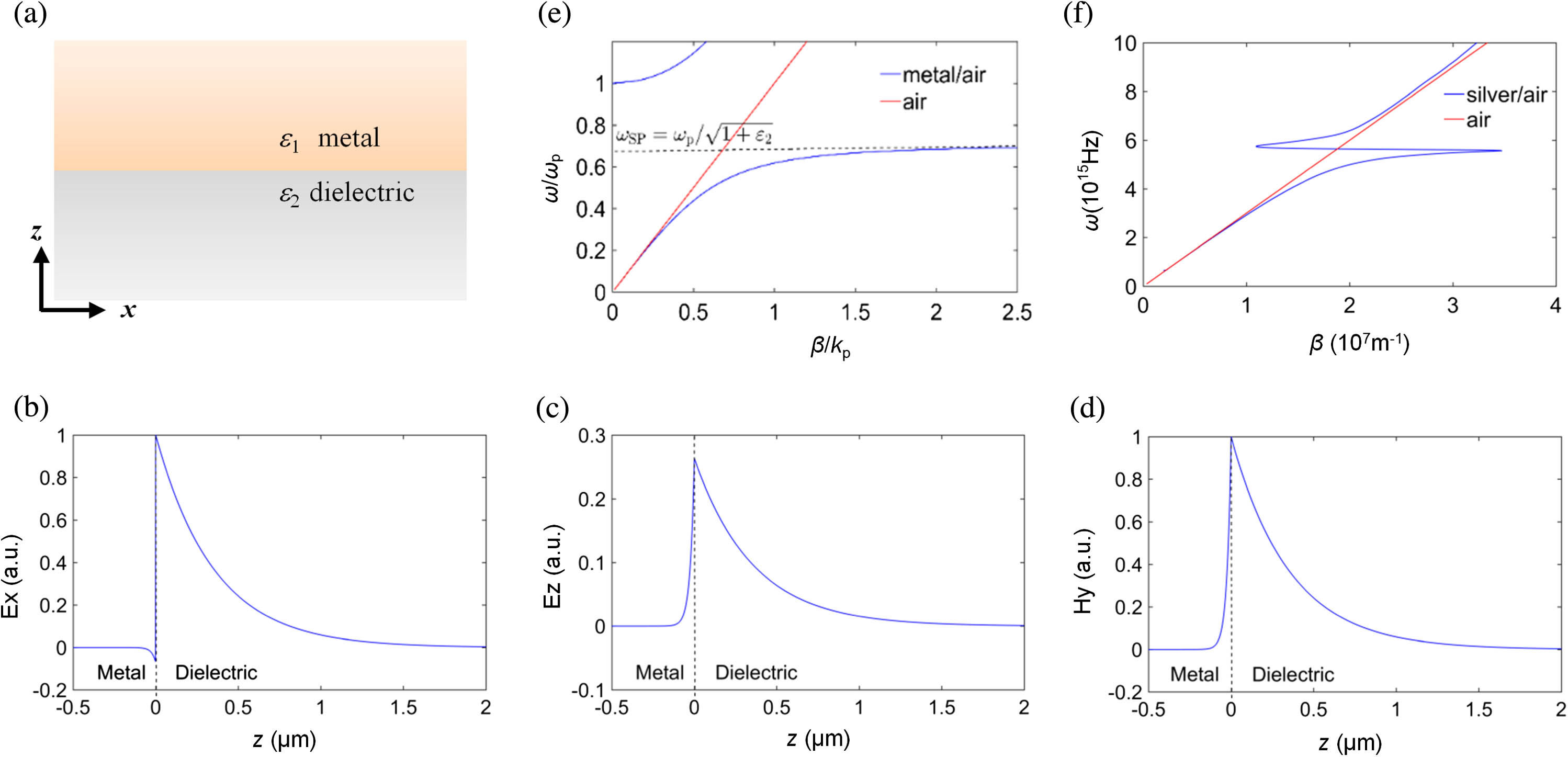
Figure 1.Surface plasmon polaritons (SPPs) characteristics. (a) Metal–dielectric interface with complex permittivities
Further utilizing boundary conditions, we can reveal the SPPs dispersion relation:
2. SPR Sensors
In order to excite SPPs at the metal–dielectric interface, phase-matching methods such as prism-coupling or grating-coupling have to be employed, since the momentum of SPPs is larger than same-energy photons in the dielectric. As shown in Fig. 2(a), in the so-called Kretschmann configuration, a prism with permittivity
![]()
Figure 2.(a) Gain-enhanced SPR resonance. SPPs at a metal–dielectric interface (Kretschmann configuration) excited by an electromagnetic wave with wave vector
The propagation constant of SPPs is sensitive to the change in the refractive index of the dielectric environment. This characteristic of SPR can be used to make sensors. In SPR sensors with angular modulation, the angle-dependent reflectivity is measured to confirm the resonant angle, and the shift of the resonant angle can be calibrated to the given refractive index. Besides angle modulation, also wavelength [27], intensity [3], phase [28], and polarization [29] modulation SPR sensors have been demonstrated.
3. Inherent Limit of SPR Sensors
The performance of SPR sensors can be quantified by sensitivity and figure of merit (FOM) [30,31]. Taking the wavelength sensing as an example, the sensitivity
B. Gain Compensates Loss
Loss limits the performance of SPR sensors. Placing a gain material close to the metal surface has been shown to be an effective strategy to compensate loss [32–38]. Here, we illustrate how gain compensates loss in conventional SPR sensors. First, we expound the compensation mechanism, and then we show the effect of gain on SPR by analytical calculation and full-wave simulation.
1. Compensation Mechanism
The interaction between photons and surface plasmons in the Kretschmann configuration can be investigated by applying Fresnel’s reflection theory to a three-layer system [4]. The angle-dependent reflectivity of incident light is
To elaborate how the loss affects the FWHM of the SPR, we simplify Eq. (5) to a Lorentzian-type function for small loss
The FWHM of the Lorentzian term in Eq. (7) is determined by the inverse of the SPPs propagation length:
2. Effect of Gain
In order to illustrate the effect of introducing gain to the dielectric, we exemplarily analyze a gain-assisted SPR sensor in the Kretschmann configuration both analytically and with a full-wave simulation. In the setup, corresponding to Fig. 2(a), the upper layer is a high refractive index prism (BK7) with permittivity
The results of the analytical calculation and full-wave simulation are shown in Figs. 2(b)–2(f). The dependence of the reflectivity on the angle of incidence and on the gain coefficient, obtained from our analytical calculations, is shown in Fig. 2(b). At zero gain, we find a dip in the angle-dependent reflectivity. When increasing the gain value, the magnitude of the dip decreases to the point where
Figure 2(c) shows the angle-dependent reflectivity at three different gain values. The solid lines correspond to analytical results, while the dotted data are acquired through the full-wave simulation. In the low-gain regime, both methods predict a spectral dip centered at 70.3 deg with an FWHM of about 4 deg. The FWHM of the reflectivity spectrum is given in Fig. 2(d) and shows a minimum near zero at a gain value of
3. Gain-Assisted SPR
Gain-assisted SPR has been theoretically investigated for more than a decade. It has been shown that through the introduction of gain, the amplified SPPs exhibit low group velocities and tight localization to the metal–dielectric interface [34]. Besides loss compensation [35], gain also poses a strong means to manipulate dispersion and propagation characteristics of electromagnetic pulses at the nanoscale [36].
Theoretical advances were soon accompanied by experimental demonstrations of gain-assisted SPR. Seidel et al. used a dye solution as gain medium for SPPs amplification [37]. Noginov et al. employed a dye embedded within a polymer matrix to achieve the sufficient optical gain
3. LESPR SENSORS
In Section 2 we have shown that by introducing gain to the SPR sensor, the linewidth of the resonance can be reduced, which translates into an enhanced sensing performance. These gain-assisted SPR sensors require (in the same way as conventional SPR sensors) phase-matching techniques in order to excite SPPs. This introduces experimental difficulties such as precise adjustment of the incidence angle in prism coupling, which hinders sensor miniaturization to the nanoscale [36–38]. This issue, however, can be avoided in the LESPR configurations. Through the introduction of a nanocavity to the system, the Purcell effect [39] arises. It describes the increase in spontaneous emission rate of emitters within a resonant cavity by the so-called Purcell factor
In 2003, David Bergman and Mark Stockman proposed the concept of a “spaser,” the acronym of surface plasmon amplification by stimulated emission of radiation [40]. Initially, the spaser is about the localized surface plasmon polariton amplifiers. Recently, this concept has been generalized to include traveling surface plasmon polariton amplifiers, or plasmonic nanolasers. In 2009, three teams demonstrated the first plasmonic nanolasers in different configurations [41–43]. Driven by the ongoing race to laser miniaturization and the great potential applications, to date, there are numerous reported plasmonic nanolasers in unique architectures; we kindly suggest the readers to refer the review articles of Refs. [44–63].
The studies of plasmonic nanolasers lead to a novel class of LESPR sensors. In this section we first present the setup and merits of the LESPR sensors. Then we review the design features of LESPR sensing devices: plasmonic and gain materials as well as feedback mechanisms. We furthermore discuss how sufficient modal overlap between SPPs and analyte is crucial for a high sensitivity.
A. Setup of LESPR Sensors
A typical LESPR sensor consists of a plasmonic laser device and corresponding pump-measurement optical system, as shown in Fig. 3(a). Comparing to the SPR device, there is an additional nanocavity providing optical feedback for lasing. When the gain material is excited with a pump laser, electron–hole pairs are created. Upon recombination, they predominantly radiate into surface plasmon modes due to the Purcell effect. When increasing pump power, gain increases until cavity losses are compensated, and lasing is acquired. In LESPR sensors, a change in the environment around the cavity, the refractive index change for instance, produces a change in the lasing characteristics. A portion of the encoded SPPs couple out into the far field and yield an output signal for readout. Figure 3(b) illustrates that LESPR is with a narrower linewidth compared to SPR, which yields superior intensity sensing performance at a given wavelength shift.
![]()
Figure 3.Lasing-enhanced surface plasmon resonance (LESPR) sensor. (a) Schematic of an LESPR sensor setup. A plasmonic nanolaser is surrounded by the liquid analyte, where the refractive index change of the analyte will shift the lasing emission wavelength. LESPR sensor has a much narrower spectral linewidth than an SPR sensor. (b) A schematic showing that, for a given resonance peak shift, the LESPR sensor has a much larger intensity change than an SPR sensor. Figure adapted [24].
B. Merits of LESPR Sensors
The merits of LESPR sensors stem from their capability to localize electromagnetic fields both in frequency and space.
C. Design Features and Recent Progress
1. Plasmonic Material
SPPs originate from the collective oscillations of free electrons. Plasmonic materials provide an abundance of free electrons which represent as a negative real permittivity. However, plasmonic materials suffer from large ohmic loss, especially in the visible and ultraviolet (UV) spectral ranges, arising from electronic interband and intraband transitions. The choice of the plasmonic material has a significant impact on the plasmonic loss that has to be overcome to achieve lasing action. In Eq. (10) we see that the loss particularly depends on the ratio of the imaginary and real parts of the complex permittivity
The most prominent materials supporting SPPs are silver (Ag), gold (Au), aluminum (Al), and copper (Cu). Above 300 nm, silver exhibits the lowest
Besides the material itself, the fabrication quality of metal films plays an important role in achieving lower ohmic loss. Epitaxial growth, for example, allows fabrication of monocrystalline, atomically smooth surfaces, allowing to reduce loss compared to earlier reports [66–68]. Aside from these metals, new plasmonic materials have been proposed which can compete with the typical metals in performance. For example, in NIR indium tin oxide and doped zinc oxides (Al:ZnO, Ga:ZnO) have a smaller
2. Gain Material
In so-far realized LESPR sensor devices, semiconductors such as CdS [23] and CdSe [24,71] nanosquares or ZnO nanorods [72] have been commonly used as gain materials. These binary II–VI semiconductors exhibit high gain and large refractive indices. They can provide gain from UV to VIS and the plasmonic lasers based on them can be operated at room temperature [64]. Organic dyes have also been used, which offer broad gain spectra ranging from UV to NIR. In solution, dyes can be easily implemented into device geometries. As a disadvantage, organic dyes are subject to photobleaching and, in high concentrations, their performance suffers from photon quenching. Through optimized pumping methods, however, these effects can be reduced.
In plasmonic nanolasers, more gain materials have been employed, such as III-V semiconductors [73,74], ternary and quaternary compound semiconductors fabricated into heterostructures and superlattices [75], as well as quantum dots [76]. Quantum dots provide confinement in all spatial dimensions yielding higher gain with tunable spectral range. Other promising gain materials to be studied in the context of LESPR are perovskites, which recently have attracted great attention in photonic devices due to their intriguing properties [64,77–81]. These gain materials may also be suitable for designing sensing devices.
3. Feedback Mechanism
An essential part in realizing a laser device is providing feedback to the system. In this section we introduce three mechanisms, namely total internal reflection, Fabry–Perot resonator, and distributed feedback, which have been employed in realized LESPR sensors. We briefly discuss how the feedback mechanisms are incorporated into the respective sensing devices. For more experimental details we advise the reader to proceed to Section 4.
In the nanosquare design by Wang et al. [24,71], feedback was implemented through the gain medium itself via total internal reflection of surface plasmons at the nanosquare boundaries [23,82–84]. Nanosquares of only tens of nanometers in thickness can still support both transverse-electric (TE) and TM waves. However, as TE waves are delocalized from the nanosquare surface (and thus carry less momentum than TM waves), they are scattered out-of-plane more strongly than TM waves. Consequently, only TM waves, i.e., SPPs, efficiently undergo total internal reflection to achieve sufficient feedback for lasing [82].
Feedback can also be provided through the introduction of a Fabry–Perot etalon as realized by Zhu et al. [85]. In their work, they used silver as plasmonic material formed into a trench. The silver trench constitutes a Fabry–Perot cavity. SPPs excited through pumping would oscillate between the facing silver surfaces which serve as SPPs mirrors [86,87].
In order to enhance the quality factor of the cavity, Cheng et al. [72] employed distributed feedback, specifically a distributed Bragg reflector (DBR) [88,89], in their nanolaser design. A DBR is a structure of periodically alternating refractive indices. In their work, Cheng et al. placed a ZnO nanowire onto a grated Al surface. The grating serves as a hybrid plasmonic Bragg reflector which increases the quality factor by reducing mirror loss at the end facets of the nanowire.
4. Overlap between Optical Field and Analyte
The sensitivity (i.e., the magnitude of the resonance shift for a given change of the refractive index) greatly depends on the modal overlap between the SPPs and the analyte. As the SPPs mode is strongly confined to the interface, there is typically only little overlap. However, through minimizing the physical volume below the diffraction limit, the field becomes delocalized from the surface. This enables an increased overlap between the field and the analyte and thus increases the sensitivity [24].
Recently, nanolasing in a gap-plasmon-mode nanocavity with an ultrasmall mode volume (
5. Distinguish a Plasmonic Mode from a Photonic Mode
Plasmonic modes and photonic modes usually coexist in a plasmonic nanolaser cavity. They can be distinguished in a few ways. First, photonic modes have larger cut-off size than plasmonic modes. So, an easy and straightforward way to construct a nanocavity with exclusive plasmonic modes is to make the cavity size smaller than the photonic mode cut-off size in certain dimensions [42,82,92]. Second, plasmonic modes and photonic modes can have different emission patterns and corresponding polarization states. For a given cavity configuration, the emission pattern and corresponding polarization state of its each eigenmode can be obtained by full-wave simulation. And thereby, direct characterization of its imaging pattern and polarization state can be used to distinguish a lasing mode [42,82,93,94]. Third, plasmonic modes and photonic modes have different group indices. For a multimode lasing device, the group index of the lasing modes can be calculated and used to distinguish the lasing mode [43,95]. Lastly, plasmonic modes and photonic modes can have different Purcell effect, which will result in different spontaneous emission lifetime [42,82,92]. And thereby lifetime characterization can help to distinguish the lasing mode.
4. APPLICATIONS
In this section we discuss so-far realized LESPR sensors with respect to their applications, namely refractive index sensing and gas detection, in more detail. In the context of biological applications, we consider pioneering experiments for biological probing, super-resolution biomedical imaging, and cellular labeling and tracking.
A. Refractive Index Sensing
In 2016, Wang et al. reported an LESPR sensor for refractive index sensing [24]. The plasmonic nanolaser consists of a CdSe nanosquare on top of an Au film separated by a few nanometers thick
![]()
Figure 4.LESPR sensor for refractive index sensing. (a) SEM image of an LESPR sensor. (b) Lasing emission from the LESPR sensor with ethanol (olive) and propyl alcohol (red) as analyte. The spectrum shifts in response to a refractive index change of
Most of the LESPR sensors realized by today are designed for refractive index sensing in solution, which is the most common application of established surface plasmon resonance sensors, particularly in the field of biosensing [4]. Refractive index sensing in solution imposes two requirements on a high-performance LESPR sensor. (i) The pump and emission beam must barely interact with the analyte. For biosensing a suitable window lies, for example, in the NIR regime (
For meeting the latter condition, surface passivation may be employed to prevent photoreactions between the analyte and gain medium. In a study, Wang et al. [71] compared the stability and yield of passivated and nonpassivated plasmonic nanolasers. They fabricated 158 plasmonic nanolasers in the same configuration as shown in Fig. 4(a), i.e., CdSe as gain medium placed, separated by a thin
![]()
Figure 5.High-yield plasmonic nanolasers with superior stability for sensing in aqueous solution. (a), (b) Continuous trace of emission spectra of CdSe nanosquare plasmonic nanolasers without and with an
The device of Cheng et al. [72] is a hybrid plasmonic crystal nanolaser consisting of a ZnO nanowire placed onto an aluminum grating surface with a nanotrench defect cavity. Figures 6(a) and 6(b) show schematics of the device. The device’s emission wavelength is 373 nm with a linewidth 0.22 nm. The grating serves as a hybrid plasmonic Bragg reflector, increasing the quality factor, while the nanotrench serves as a sensing cavity in which the resonant modes are strongly confined. In this way, the sensitivity is enhanced as the overlap between the SPP mode and the analyte is increased. Figures 6(c) and 6(d) show the mode profile for different trench depths. Through optimizing the device’s structural parameters for best performance, they achieved an FOM of 1132 for refractive index sensing of glucose in their simulations. The sensitivity as well as the transparency threshold gain in dependence of the cavity depth is depicted in Fig. 6(e).
![]()
Figure 6.Plasmonic nanolasers with a nanotrench defect cavity for sensing applications. (a) Schematic of a plasmonic nanolaser with a nanotrench defect. (b) Schematic of the plasmonic nanolaser with a nanotrench defect for glucose solution sensing. (c), (d) Side view of resonant mode profiles
Zhu et al. [85] investigated the lasing performance of a metallic trench plasmonic laser and analyzed its sensing performance theoretically. The cavity floor is coated with PMMA:DCM as dye gain medium. Through pumping the gain medium with blue–green light, SPPs are excited and resonate between the silver surfaces. Figure 7(a) shows a schematic of the structure. In order to convert the SPPs into propagating light, an off-centered slit is incorporated into the outside of the cavity floor. Zhu et al. increased the pump efficiency by adding a sinusoidal grating to the cavity floor. An SEM image of the grated cavity floor is depicted in Fig. 7(b). Through the grating, the pump light is first converted into SPPs confined to the cavity floor which subsequently pump the gain medium. Under normal incidence, pulsed laser illumination with
![]()
Figure 7.Plasmonic laser based on a metallic trench Fabry–Perot resonator. (a) Schematic of the device consisting of a silver trench. The cavity floor of length
B. Gas Detection
In 2014, Ma et al. [23] realized an LESPR sensor to detect trace level explosives in air. They used a CdS nanosquare atop of Ag, separated by
![]()
Figure 8.Plasmonic nanolaser for gas detection. (a) Schematic of the detector consisting of a semiconductor nanosquare on top of a
In 2007, Melentiev et al. [98] demonstrated an intracavity LESPR sensor using a plasmonic laser created from a periodically perforated silver film with a liquid gain medium (a R101 dye in dimethyl sulfoxide). With this device, they were able to detect analyte concentrations down to 0.07 ppm (parts per million) in solution.
C. Biological Applications
Over the decades, SPR sensors have developed into a commercial tool to research biomolecular interactions and detect biological analytes related to environmental monitoring, food safety and security, and medical diagnostics [4]. SPR sensors have been refined to the stage where they can be used for detecting biomolecules in clinical samples. Recent examples include the detection of proteins [99–107], antibodies [108], hormones [109,110], DNA [111,112], and microRNA [113–118].
All of the above-mentioned SPR and LESPR sensors are based on propagating SPPs and have physical dimensions at scale of several hundred nanometers and above. Sensors of these dimensions are unsuitable to insert into cells as they would damage the cells. However, plasmonic nanolasers based on localized surface plasmons can be as small as tens of nanometers, which render them potential candidates for intracellular applications.
1. Biological Probe
In 2017, Galanzha et al. [91] experimentally demonstrated a 22 nm plasmonic nanolaser serving as a bright, water-soluble, and biocompatible probe that exhibits stimulated emission directly inside living cells and animal tissue. The demonstrated spaser has a more than 100 times brighter emission intensity and a 30-fold narrower spectral width compared to quantum dots, which are currently among the best conventional fluorescence probes.
The spaser consists of a spherical gold nanoparticle (similar to nanoparticles commonly used in the biomedical field) surrounded by a silica shell with an uranine dye (which is widely used for tracing and biomedical diagnostics thanks to low toxicity and high solubility in water and physiological solution). Figure 9(a) shows a schematic of the spaser. In order to target cancer cells, the spasers are conjugated with folic acid. The corresponding folate receptor is commonly overexpressed on the surface of human cancer cells in comparison to normal cells. Because of that, a higher concentration of spasers forms at the surface of cancer cells, which, in turn, yields contrast in imaging. Figures 9(c) and 9(d) show fluorescence images of breast cancer cells (MDA-MB-231) with a single and multiple spasers bound to it, respectively.
![]()
Figure 9.Spaser as biological probes. (a) Spaser schematic. (b) Stimulated emission of spasers in suspension. Light–light curve (red) and emission linewidth in dependence of pump fluence (blue). At about
The spasers serve as multimodal contrast agents as they can not only be exploited for optical, but also photoacoustic (PA) and photothermal (PT) imaging, as shown in Fig. 9(a). After optical excitation of the spasers, some of the energy is dissipated thermally, which leads to the formation of bubbles and consequently acoustic waves, as illustrated in Fig. 9(b). As the bubbles are formed, the spasers’ dielectric polarizability is reduced, which causes the plasmonic eigenmode’s frequency to increase, shifting it closer to the transition energy of the gain medium. This leads to a significantly increased number of plasmons in the spasing mode, increasing the emission intensity. In this work, the phenomenon is referred to as “nanobubble giant spasing.” In Fig. 9(b), “giant spasing” is indicated by a rapid increase in emission intensity at a pump pulse fluence of
Furthermore, Galanzha et al. show that with a combination of PA diagnosis and PT therapy (PA-PT spaser theragnostics), only a few laser pulses are necessary to destroy cancer cells. The demonstrated spaser, in this way, contributes to the promising field of spaser-based therapeutic applications and high-contrast imaging with low photobleaching in vitro and in vivo at the single-cell level, with pump intensities that agree with laser safety standards.
2. STED Super-Resolution Imaging
Recently, the concept of spaser-based stimulated emission depletion (STED) super-resolution microscopy has been demonstrated and its feasibility has been investigated [119]. The idea of STED is utilizing stimulated emission to inhibit spontaneous fluorescent emission in a specific spatial region [120]. In a real implementation, a pumping pulse creates a population inversion and a following depletion pulse causes stimulated emission which depletes the population inversion. Both pulses are focused to the objects labeled by fluorescent dyes. The depleting pulse has a donut shape in the focus, and the undepleted area at the center of the shape is significantly smaller than the wavelength, allowing for the super-resolution microscopy.
A similar principle is applied to spaser-based STED which uses a depletion beam to switch-off the spasing action, as shown in Fig. 10(a). The super-resolution is evident by comparing of confocal and STED imaging, as depicted in Figs. 10(c) and 10(d). As shown in Fig. 10(e), the resolution of confocal in the magenta box is 286 nm, whereas that of the spaser-STED is 74 nm. Moreover, the dependence of imaging resolution on depletion power validated the feasibility of STED super-resolution on spaser nanoparticles. Besides spatial super-resolution, the most significant advantage of spaser-STED is spectral confinement. The ultranarrow linewidth of spasing [3.8 nm, as shown in Fig. 10(b)] enables a narrowband STED imaging with an acquisition bandwidth of 10 nm, which could be a possible solution to the spectral cross talk issue in the common spontaneous fluorescent emission based (STED) instruments. These spaser nanoparticles in principle allow for spectral-multiplexed biomedical imaging and other applications.
![]()
Figure 10.Spaser for ultranarrow bandwidth STED super-resolution imaging. (a) Principle of STED of spaser radiation. (b) Spectra of fluorescent dyes (dashed red line) and spaser nanoparticles (solid black line). Inset shows transmission electron microscope image of the spaser. (c) Confocal and (d) STED images of separated single spasers. (e) Intensity profile on the dashed magenta line (confocal) and solid line (STED) box. The fitted lines indicate the resolutions are 286 nm (confocal) and 74 nm (STED) by FWHM. (f) Measured resolution enhancement by increasing STED depletion power. Figure adapted [119].
3. Cellular Labeling and Tracking
Due to the large cellular heterogeneity in biological systems, large-scale single cell analyses have become increasingly important. For this matter, fluorescence-based approaches can only differ between small numbers of specific cells because of spectral cross talk between conventional fluorophores. The use of photonic microdisk lasers, however, enables massive spectral multiplexing thanks to their wide tunability and narrow linewidth lasing emission.
In a recent work from 2019, Martino et al. [121] investigated large-scale cell tracking using intracellular laser particles as imaging probes. The used photonic microdisk lasers consist of InAlGaAs and InGaAsP quaternary semiconductors (with bandgaps in the NIR-II window) cut into disks of about 2 μm in diameter using electron-beam lithography, as shown in Fig. 11(a). In this diameter range, the emission wavelength changes about 1 nm per nanometer change in the disk’s diameter. They allow the disk diameters to vary by about 200 nm in fabrication such that the microdisks exhibit emission wavelengths spreading over the gain spectrum of the respective semiconductor. In this way, they fabricate hundreds of lasing nanoparticles with emission maxima ranging from 1180 nm to 1580 nm spaced by about 1 nm.
![]()
Figure 11.Microdisk laser particles for cellular labeling and tracking. (a) SEM image of silica-coated CLPs. Top left: false-color cross-sectional SEM image of a coated microdisk cut with focused ion beam. (b) Confocal fluorescence image of mouse breast tumor (4T1) cells with staining for actin (magenta), and nucleus (green), overlaid with bright-field transmission image of LPs (gray scale). (c) Overlaid LASE-fluorescence image of LPs inside membrane-GFP-expressing human embryonic kidney (HEK-293) cells. Inset, zoomed-in images of three LPs, in which the color of each dot (pixel) represents the peak wavelength of laser emission. (d) SEM image of an array of OLPs on pillars. Top left: SEM image of an OLP after detachment. (e), (f) Slope efficiency versus orientation angle
To enable operation in aqueous solution, the nanoparticles are passivated through coating with silicon dioxide. This avoids corrosion and also allows to functionalize the particles, e.g., for multimodal imaging, biomolecule sensing, or cell-type-specific targeting. Martino et al. demonstrated large-scale cell tracking using polyclonal 4T1 breast cancer cells tagged with the above-mentioned laser particles, as shown in Fig. 11(b). Using a compact cell-culture incubator on the microscope, they acquired time-lapse LASE images of laser particles (LPs) inside cells, as shown in Fig. 11(c). The cancer cells are modeled into a three-dimensional tumor spheroid, which contains about 70,000 lasing particles. With their stimulated emission microscopy setup and tracking algorithm, they were able to track 75%–80% of all detected laser particles for longer than 24 h, of which 731 were tracked for more than 125 h. They achieved real-time tracking of thousands of individual cells in the tumor model over several days, revealing different behavioral phenotypes.
However, the far-field emission of whispering gallery mode in laser particle is predominantly in the plane of the cavity resonance direction. During tracking, the orientations of the particles vary randomly inside cells; therefore, the measured laser signal is randomly fluctuated and frequently lost. Recently, omnidirectional emission from microdisk laser particles by incorporating light scattering into the cavity has been demonstrated [122]. As shown in Fig. 11(d), these laser particles could be realized by coating the microdisks with silicon nanoparticles with a large refractive index but low absorption loss. Significantly more lasing light was collected from omnidirectional laser particles (OLPs) than from conventional laser particles (CLPs), as evidenced by the increased slope or “slope efficiency” of the input–output curve above the threshold, as shown in Figs. 11(e) and 11(f). The minimum-to-maximum ratio of the angle-dependent laser output intensity is improved from 0.007 to
5. CONCLUSION AND OUTLOOK
In this paper, we summarize the fundamental properties and review the recent progress of LESPR sensors. The review focuses primarily on the basic physical mechanisms, design features, and applications. We see the exotic characteristics of LESPR sensors: the gain compensates the loss leading to a narrow-linewidth lasing emission and the direct excitation of SPPs without the phase match setup leading to a compact device size. Being able to generate coherent and nanolocalized optical fields, LESPR sensors integrate the advantages of both LSPs and propagating SPPs based sensors and improve their deficiencies, which enables them a novel class of label-free sensors with high performance. Convincing demonstrations have been reported for applications in refractive index sensing, analyte concentration detection, and biological diagnosis. However, many research efforts have to be conducted to forge LESPR sensors as a mature sensing technology. As potentially productive follow-up steps we identify the exploration of more sensor designs, drawing from the diversity of already realized plasmonic laser designs that have not been tested in sensing applications yet. In particular, cavity configuration engineering and metal quality improvements are crucial. Some proven techniques used in the commercial SPR sensors have yet to be exploited, such as large-area integration of sensor arrays and chemical surface treatment. Regarding biomedical applications, we consider it worthy to further explore plasmonic nanolasers for labeling and tracking, as they may constitute superior agents for highly multiplexed cell tagging and tracking among other applications, due to their strong spatial and spectral localization capability.
References
[1] S. A. Maier. Plasmonics: Fundamentals and Applications(2007).
[2] C. Nylander, B. Liedberg, T. Lind. Gas detection by means of surface plasmon resonance. Sens. Actuators, 3, 79-88(1982).
[3] B. Liedberg, C. Nylander, I. Lunström. Surface plasmon resonance for gas detection and biosensing. Sens. Actuators, 4, 299-304(1983).
[4] J. Homola, J. Dostálek. Surface Plasmon Resonance Based Sensors(2006).
[5] J. Homola, S. S. Yee, G. Gauglitz. Surface plasmon resonance sensors: review. Sens. Actuators B, 54, 3-15(1999).
[6] J. Zhou, Q. Qi, C. Wang, Y. Qian, G. Liu, Y. Wang, L. Fu. Surface plasmon resonance (SPR) biosensors for food allergen detection in food matrices. Biosens. Bioelectron., 142, 111449(2019).
[7] M. E. Stewart, C. R. Anderton, L. B. Thompson, J. Maria, S. K. Gray, J. A. Rogers, R. G. Nuzzo. Nanostructured plasmonic sensors. Chem. Rev., 108, 494-521(2008).
[8] J. N. Anker, W. P. Hall, O. Lyandres, N. C. Shah, J. Zhao, R. P. Van Duyne. Biosensing with plasmonic nanosensors. Nat. Mater., 7, 442-453(2008).
[9] A. J. Haes, R. P. Van Duyne. A unified view of propagating and localized surface plasmon resonance biosensors. Anal. Bioanal. Chem., 379, 920-930(2004).
[10] M. I. Stockman. Nanoplasmonic sensing and detection. Science, 348, 287-288(2015).
[11] G. J. Nusz, A. C. Curry, S. M. Marinakos, A. Wax, A. Chilkoti. Rational selection of gold nanorod geometry for label-free plasmonic biosensors. ACS Nano, 3, 795-806(2009).
[12] E. Cubukcu, S. Zhang, Y.-S. Park, G. Bartal, X. Zhang. Split ring resonator sensors for infrared detection of single molecular monolayers. Appl. Phys. Lett., 95, 043113(2009).
[13] G. Peng, U. Tisch, O. Adams, M. Hakim, N. Shehada, Y. Y. Broza, S. Billan, R. Abdah-Bortnyak, A. Kuten, H. Haick. Diagnosing lung cancer in exhaled breath using gold nanoparticles. Nat. Nanotechnol., 4, 669-673(2009).
[14] A. V. Kabashin, P. Evans, S. Pastkovsky, W. Hendren, G. A. Wurtz, R. Atkinson, R. Pollard, V. A. Podolskiy, A. V. Zayats. Plasmonic nanorod metamaterials for biosensing. Nat. Mater., 8, 867-871(2009).
[15] J.-F. Li, Y.-F. Huang, Y. Ding, Z.-L. Yang, S.-B. Li, X.-S. Zhou, F.-R. Fan, W. Zhang, Z.-Y. Zhou, D.-Y. Wu, B. Ren, Z.-L. Wang, Z.-Q. Tian. Shell-isolated nanoparticle-enhanced Raman spectroscopy. Nature, 464, 392-395(2010).
[16] A. A. Yanik, M. Huang, O. Kamohara, A. Artar, T. W. Geisbert, J. H. Connor, H. Altug. An optofluidic nanoplasmonic biosensor for direct detection of live viruses from biological media. Nano Lett., 10, 4962-4969(2010).
[17] A. A. Yanik, A. E. Cetin, M. Huang, A. Artar, S. H. Mousavi, A. Khanikaev, J. H. Connor, G. Shvets, H. Altug. Seeing protein monolayers with naked eye through plasmonic Fano resonances. Proc. Natl. Acad. Sci. USA, 108, 11784-11789(2011).
[18] N. Liu, M. L. Tang, M. Hentschel, H. Giessen, A. P. Alivisatos. Nanoantenna-enhanced gas sensing in a single tailored nanofocus. Nat. Mater., 10, 631-636(2011).
[19] A. G. Brolo. Plasmonics for future biosensors. Nat. Photonics, 6, 709-713(2012).
[20] V. R. Dantham, S. Holler, C. Barbre, D. Keng, V. Kolchenko, S. Arnold. Label-free detection of single protein using a nanoplasmonic-photonic hybrid microcavity. Nano Lett., 13, 3347-3351(2013).
[21] N. Li, A. Tittl, S. Yue, H. Giessen, C. Song, B. Ding, N. Liu. DNA-assembled bimetallic plasmonic nanosensors. Light Sci. Appl., 3, e226(2014).
[22] K. M. Mayer, J. H. Hafner. Localized surface plasmon resonance sensors. Chem. Rev., 111, 3828-3857(2011).
[23] R.-M. Ma, S. Ota, Y. Li, S. Yang, X. Zhang. Explosives detection in a lasing plasmon nanocavity. Nat. Nanotechnol., 9, 600-604(2014).
[24] X.-Y. Wang, Y.-L. Wang, S. Wang, B. Li, X.-W. Zhang, L. Dai, R.-M. Ma. Lasing enhanced surface plasmon resonance sensing. Nanophotonics, 6, 472-478(2017).
[25] A. Shalabney, I. Abdulhalim. Sensitivity enhancement methods for surface plasmon sensors. Laser Photonics Rev., 5, 571-606(2011).
[26] E. T. Arakawa, M. W. Williams, R. N. Hamm, R. H. Ritchie. Effect of damping on surface plasmon dispersion. Phys. Rev. Lett., 31, 1127-1129(1973).
[27] L. Zhang, D. Uttamchandani. Optical chemical sensing employing surface plasmon resonance. Electron. Lett., 24, 1469-1470(1988).
[28] J. M. Brockman, B. P. Nelson, R. M. Corn. Surface plasmon resonance imaging measurements of ultrathin organic films. Annu. Rev. Phys. Chem., 51, 41-63(2000).
[29] A. A. Kruchinin, Y. G. Vlasov. Surface plasmon resonance monitoring by means of polarization state measurement in reflected light as the basis of a DNA-probe biosensor. Sens. Actuators B, 30, 77-80(1996).
[30] P. Berini. Figures of merit for surface plasmon waveguides. Opt. Express, 14, 13030-13042(2006).
[31] M. A. Otte, B. Sepúlveda, W. Ni, J. P. Juste, L. M. Liz-Marzán, L. M. Lechuga. Identification of the optimal spectral region for plasmonic and nanoplasmonic sensing. ACS Nano, 4, 349-357(2010).
[32] S. P. Ng, Y. Y. Yip, C. M. L. Wu. Biosensing with gain-assisted surface plasmon-polariton amplifier: a computational investigation. Sens. Actuators B, 210, 36-45(2015).
[33] M. A. Noginov, V. A. Podolskiy, G. Zhu, M. Mayy, M. Bahoura, J. A. Adegoke, B. A. Ritzo, K. Reynolds. Compensation of loss in propagating surface plasmon polariton by gain in adjacent dielectric medium. Opt. Express, 16, 1385-1392(2008).
[34] I. Avrutsky. Surface plasmons at nanoscale relief gratings between a metal and a dielectric medium with optical gain. Phys. Rev. B, 70, 155416(2004).
[35] M. P. Nezhad, K. Tetz, Y. Fainman. Gain assisted propagation of surface plasmon polaritons on planar metallic waveguides. Opt. Express, 12, 4072-4079(2004).
[36] A. A. Govyadinov, V. A. Podolskiy. Gain-assisted slow to superluminal group velocity manipulation in nanowaveguides. Phys. Rev. Lett., 97, 223902(2006).
[37] J. Seidel, S. Grafström, L. Eng. Stimulated emission of surface plasmons at the interface between a silver film and an optically pumped dye solution. Phys. Rev. Lett., 94, 177401(2005).
[38] M. A. Noginov, G. Zhu, M. Mayy, B. A. Ritzo, N. Noginova, V. A. Podolskiy. Stimulated emission of surface plasmon polaritons. Phys. Rev. Lett., 101, 226806(2008).
[39] E. Purcell. Spontaneous emission probabilities at radio frequencies. Phys. Rev., 69, 681(1946).
[40] D. J. Bergman, M. I. Stockman. Surface plasmon amplification by stimulated emission of radiation: quantum generation of coherent surface plasmons in nanosystems. Phys. Rev. Lett., 90, 027402(2003).
[41] M. A. Noginov, G. Zhu, A. M. Belgrave, R. Bakker, V. M. Shalaev, E. E. Narimanov, S. Stout, E. Herz, T. Suteewong, U. Wiesner. Demonstration of a spaser-based nanolaser. Nature, 460, 1110-1112(2009).
[42] R. F. Oulton, V. J. Sorger, T. Zentgraf, R.-M. Ma, C. Gladden, L. Dai, G. Bartal, X. Zhang. Plasmon lasers at deep subwavelength scale. Nature, 461, 629-632(2009).
[43] M. T. Hill, M. Marell, E. S. P. Leong, B. Smalbrugge, Y. Zhu, M. Sun, P. J. van Veldhoven, E. J. Geluk, F. Karouta, Y.-S. Oei, R. Notzel, C.-Z. Ning, M. K. Smit. Lasing in metal-insulator-metal sub-wavelength plasmonic waveguides. Opt. Express, 17, 11107-11112(2009).
[44] P. Berini, I. De Leon. Surface plasmon–polariton amplifiers and lasers. Nat. Photonics, 6, 16-24(2012).
[45] R.-M. Ma, R. F. Oulton, V. J. Sorger, X. Zhang. Plasmon lasers: coherent light source at molecular scales. Laser Photonics Rev., 7, 1-21(2013).
[46] M. T. Hill, M. C. Gather. Advances in small lasers. Nat. Photonics, 8, 908-918(2014).
[47] S. Gwo, C. K. Shih. Semiconductor plasmonic nanolasers: current status and perspectives. Rep. Prog. Phys., 79, 086501(2016).
[48] D. Wang, W. Wang, M. P. Knudson, G. C. Schatz, T. W. Odom. Structural engineering in plasmon nanolasers. Chem. Rev., 118, 2865-2881(2018).
[49] X.-W. Liu, P.-F. Xu, Y.-P. Wu, Z.-Y. Yang, C. Meng, W.-S. Yang, J.-B. Li, D.-L. Wang, X. Liu, Q. Yang. Control, optimization and measurement of parameters of semiconductor nanowires lasers. Nano Energy, 14, 340-354(2015).
[50] Y. Liang, C. Li, Y.-Z. Huang, Q. Zhang. Plasmonic nanolasers in on-chip light sources: prospects and challenges. ACS Nano, 14, 14375-14390(2020).
[51] M. I. Stockman. “Brief history of spaser from conception to the future. Adv. Photonics, 2, 054002(2020).
[52] K. Ding, C.-Z. Ning. Metallic subwavelength-cavity semiconductor nanolasers. Light Sci. Appl., 1, e20(2012).
[53] R. F. Oulton. Surface plasmon lasers: sources of nanoscopic light. Mater. Today, 15, 26-34(2012).
[54] Y. Yin, T. Qiu, J.-Q. Li, P. K. Chu. Plasmonic nano-lasers. Nano Energy, 1, 25-41(2012).
[55] Z. Wang, X. Meng, A. V. Kildishev, A. Boltasseva, V. M. Shalaev. Nanolasers enabled by metallic nanoparticles: from spasers to random lasers. Laser Photonics Rev., 11, 1700212(2017).
[56] A. Yang, D. Wang, W. Wang, T. W. Odom. Coherent light sources at the nanoscale. Annu. Rev. Phys. Chem., 68, 83-99(2017).
[57] M. I. Stockman, K. Kneipp, S. I. Bozhevolnyi, S. Saha, A. Dutta, J. Ndukaife, N. Kinsey, H. Reddy, U. Guler, V. M. Shalaev, A. Boltasseva, B. Gholipour, H. N. S. Krishnamoorthy, K. F. MacDonald, C. Soci, N. I. Zheludev, V. Savinov, R. Singh, P. Groß, C. Lienau, M. Vadai, M. L. Solomon, D. R. Barton III, M. Lawrence, J. A. Dionne, S. V. Boriskina, R. Esteban, J. Aizpurua, X. Zhang, S. Yang, D. Wang, W. Wang, T. W. Odom, N. Accanto, P. M. de Roque, I. M. Hancu, L. Piatkowski, N. F. van Hulst, M. F. Kling. Roadmap on plasmonics. J. Opt., 20, 043001(2018).
[58] M. T. Hill. Electrically pumped metallic and plasmonic nanolasers. Chin. Phys. B, 27, 114210(2018).
[59] Y.-H. Chou, C.-J. Chang, T.-R. Lin, T.-C. Lu. Surface plasmon polariton nanolasers: coherent light sources for new applications. Chin. Phys. B, 27, 114208(2018).
[60] R.-M. Ma, R. F. Oulton. Applications of nanolasers. Nat. Nanotechnol., 14, 12-22(2019).
[61] C.-Z. Ning. Semiconductor nanolasers and the size-energy-efficiency challenge: a review. Adv. Photonics, 1, 014002(2019).
[62] S. I. Azzam, A. V. Kildishev, R.-M. Ma, C.-Z. Ning, R. Oulton, V. M. Shalaev, M. I. Stockman, J.-L. Xu, X. Zhang. Ten years of spasers and plasmonic nanolasers. Light Sci. Appl., 9, 90(2020).
[63] S. S. Deka, S. Jiang, S. H. Pan, Y. Fainman. Nanolaser arrays: toward application-driven dense integration. Nanophotonics, 10, 149-169(2021).
[64] H. Wu, Y. Gao, P. Xu, X. Guo, P. Wang, D. Dai, L. Tong. Plasmonic nanolasers: Pursuing extreme lasing conditions on nanoscale. Adv. Opt. Mater., 7, 1900334(2019).
[65] P. B. Johnson, R. W. Christy. Optical constants of the noble metals. Phys. Rev. B, 6, 4370-4379(1972).
[66] K. M. McPeak, S. V. Jayanti, S. J. P. Kress, S. Meyer, S. Iotti, A. Rossinelli, D. J. Norris. Plasmonic films can easily be better: rules and recipes. ACS Photonics, 2, 326-333(2015).
[67] C.-W. Cheng, Y.-J. Liao, C.-Y. Liu, B.-H. Wu, S. S. Raja, C.-Y. Wang, X. Li, C.-K. Shih, L.-J. Chen, S. Gwo. Epitaxial aluminum-on-sapphire films as a plasmonic material platform for ultraviolet and full visible spectral regions. ACS Photonics, 5, 2624-2630(2018).
[68] Y. Wu, C. Zhang, N. M. Estakhri, Y. Zhao, J. Kim, M. Zhang, X.-X. Liu, G. K. Pribil, A. Alu, C.-K. Shih, X. Li. Intrinsic optical properties and enhanced plasmonic response of epitaxial silver. Adv. Mater., 26, 6106-6110(2014).
[69] G. V. Naik, J. Kim, A. Boltasseva. Oxides and nitrides as alternative plasmonic materials in the optical range. Opt. Mater. Express, 1, 1090-1099(2011).
[70] G. V. Naik, J. L. Schroeder, X. Ni, A. V. Kildishev, T. D. Sands, A. Boltasseva. Titanium nitride as a plasmonic material for visible and near-infrared wavelengths. Opt. Mater. Express, 2, 478-489(2012).
[71] S. Wang, B. Li, X.-Y. Wang, H.-Z. Chen, Y.-L. Wang, X.-W. Zhang, L. Dai, R.-M. Ma. High-yield plasmonic nanolasers with superior stability for sensing in aqueous solution. ACS Photonics, 4, 1355-1360(2017).
[72] P.-J. Cheng, Z.-T. Huang, J.-H. Li, B.-T. Chou, Y.-H. Chou, W.-C. Lo, K.-P. Chen, T.-C. Lu, T.-R. Lin. High-performance plasmonic nanolasers with a nanotrench defect cavity for sensing applications. ACS Photonics, 5, 2638-2644(2018).
[73] K. L. Shaklee, R. E. Nahory, R. F. Leheny. Optical gain in semiconductors. J. Lumin., 7, 284-309(1973).
[74] Y.-J. Lu, C.-Y. Wang, J. Kim, H.-Y. Chen, M.-Y. Lu, Y.-C. Chen, W.-H. Chang, L.-J. Chen, M.-I. Stockman, C. K. Shih, S. Gwo. All-color plasmonic nanolasers with ultralow thresholds: autotuning mechanism for single-mode lasing. Nano Lett., 14, 4381-4388(2014).
[75] Y. Zhang, J. Wu, M. Aagesen, H. Liu. III–V nanowires and nanowire optoelectronic devices. J. Phys. D, 48, 463001(2015).
[76] V. I. Klimov, A. A. Mikhailovsky, S. Xu, A. Malko, J. A. Hollingsworth, C. A. Leatherdale, H. J. Eisler, M. G. Bawendi. Optical gain and stimulated emission in nanocrystal quantum dots. Science, 290, 314-317(2000).
[77] S. D. Stranks, H. J. Snaith. Metal-halide perovskites for photovoltaic and light-emitting devices. Nat. Nanotechnol., 10, 391-402(2015).
[78] B. R. Sutherland, E. H. Sargent. Perovskite photonic sources. Nat. Photonics, 10, 295-302(2016).
[79] S. A. Veldhuis, P. P. Boix, N. Yantara, M. Li, T. C. Sum, N. Mathews, S. G. Mhaisalkar. Perovskite materials for light-emitting diodes and lasers. Adv. Mater., 28, 6804-6834(2016).
[80] B. R. Sutherland, S. Hoogland, M. M. Adachi, P. Kanjanaboos, C. T. O. Wong, J. J. McDowell, J. Xu, O. Voznyy, Z. Ning, A. J. Houtepen, E. H. Sargen. Perovskite thin films via atomic layer deposition. Adv. Mater., 27, 53-58(2015).
[81] Q. Zhang, R. Su, W.-N. Du, X.-F. Liu, L.-Y. Zhao, S. T. Ha, Q.-H. Xiong. Advances in small perovskite based lasers. Small Methods, 1, 1700163(2017).
[82] R.-M. Ma, R. F. Oulton, V. J. Sorger, G. Bartal, X. Zhang. Room-temperature sub-diffraction-limited plasmon laser by total internal reflection. Nat. Mater., 10, 110-113(2011).
[83] W.-H. Guo, Y.-Z. Huang, Q.-Y. Lu, L.-J. Yu. Modes in square resonators. IEEE J. Quantum Electron., 39, 1563-1566(2003).
[84] Y.-Z. Huang, K.-J. Che, Y.-D. Yang, S.-J. Wang, Y. Du, Z.-C. Fan. Directional emission InP/GaInAsP square-resonator microlasers. Opt. Lett., 33, 2170-2172(2008).
[85] W. Zhu, T. Xu, H. Wang, C. Zhang, P. B. Deotare, A. Agrawal, H. J. Lezec. Surface plasmon polariton laser based on a metallic trench Fabry-Perot resonator. Sci. Adv., 3, e1700909(2017).
[86] V. J. Sorger, R. F. Oulton, J. Yao, G. Bartal, X. Zhang. Plasmonic Fabry-Pérot nanocavity. Nano Lett., 9, 3489-3493(2009).
[87] S. J. P. Kress, F. V. Antolinez, P. Richner, S. V. Jayanti, D. K. Kim, F. Prins, A. Riedinger, M. P. C. Fischer, S. Meyer, K. M. McPeak, D. Poulikakos, D. J. Norris. Wedge waveguides and resonators for quantum plasmonics. Nano Lett., 15, 6267-6275(2015).
[88] A. Hosseini, Y. Massoud. A low-loss metal-insulator-metal plasmonic Bragg reflector. Opt. Express, 14, 11318-11323(2006).
[89] J.-Q. Liu, L.-L. Wang, M.-D. He, W.-Q. Huang, D. Wang, B.-S. Zou, S. Wen. A wide bandgap plasmonic Bragg reflector. Opt. Express, 16, 4888-4894(2008).
[90] Y.-H. Hsieh, B.-W. Hsu, K.-N. Peng, K.-W. Lee, C. W. Chu, S.-W. Chang, H.-W. Lin, T.-J. Yen, Y.-J. Lu. Perovskite quantum dot lasing in a gap-plasmon nanocavity with ultralow threshold. ACS Nano, 14, 11670-11676(2020).
[91] E. I. Galanzha, R. Weingold, D. A. Nedosekin, M. Sarimollaoglu, J. Nolan, W. Harrington, A. S. Kuchyanov, R. G. Parkhomenko, F. Watanabe, Z. Nima, A. S. Biris, A. I. Plekhanov, M. I. Stockman, V. P. Zharov. Spaser as a biological probe. Nat. Commun., 8, 15528(2017).
[92] S. Wang, X.-Y. Wang, B. Li, H.-Z. Chen, Y.-L. Wang, L. Dai, R. F. Oulton, R.-M. Ma. Unusual scaling laws for plasmonic nanolasers beyond the diffraction limit. Nat. Commun., 8, 1889(2017).
[93] H.-Z. Chen, J.-Q. Hu, S. Wang, B. Li, X.-Y. Wang, Y.-L. Wang, L. Dai, R.-M. Ma. Imaging the dark emission of spasers. Sci. Adv., 3, e1601962(2017).
[94] H.-Z. Chen, S. Wang, R.-M. Ma. Characterization of plasmonic nanolasers in spatial, momentum, and frequency spaces. IEEE J. Quantum Electron., 54, 7200307(2018).
[95] Y. Wang, J. Yu, Y.-F. Mao, J. Chen, S. Wang, H.-Z. Chen, Y. Zhang, S.-Y. Wang, X.-J. Chen, T. Li, L. Zhou, R.-M. Ma, S.-N. Zhu, W.-S. Cai, J. Zhu. Stable, high-performance sodium-based plasmonic devices in the near infrared. Nature, 581, 401-405(2020).
[96] R. Weissleder. A clearer vision for
[97] J. Sun, T. Wang, Z. Jafari, F. Gao, X. Lin, H. Chen, G. Wang, I. De Leon. High-
[98] P. Melentiev, A. Kalmykov, A. Gritchenko, A. Afanasiev, V. Balykin, A. S. Baburin, E. Ryzhova, I. Filippov, I. A. Rodionov, I. A. Nechepurenko, A. V. Dorofeenko, I. Ryzhikov, A. P. Vinogradov, A. A. Zyablovsky, E. S. Andrianov, A. A. Lisyansky. Plasmonic nanolaser for intracavity spectroscopy and sensorics. Appl. Phys. Lett., 111, 213104(2017).
[99] U. Eletxigerra, J. Martinez-Perdiguero, R. Barderas, J. M. Pingarrón, S. Campuzano, S. Merino. Surface plasmon resonance immunosensor for ErbB2 breast cancer biomarker determination in human serum and raw cancer cell lysates. Anal. Chim. Acta, 905, 156-162(2016).
[100] S. K. Vashist, E. M. Schneider, J. H. T. Luong. Surface plasmon resonance-based immunoassay for human fetuin A. Analyst, 139, 2237-2242(2014).
[101] R. Wang, A. Lajevardi-Khosh, S. Choi, J. Chae. Regenerative surface plasmon resonance (SPR) biosensor: real-time measurement of fibrinogen in undiluted human serum using the competitive adsorption of proteins. Biosens. Bioelectron., 28, 304-307(2011).
[102] Y. Uludag, I. E. Tothill. Cancer biomarker detection in serum samples using surface plasmon resonance and quartz crystal microbalance sensors with nanoparticle signal amplification. Anal. Chem., 84, 5898-5904(2012).
[103] K. Pimková, M. Bocková, K. Hegnerová, J. Suttnar, J. Čermák, J. Homola, J. E. Dyr. Surface plasmon resonance biosensor for the detection of VEGFR-1—a protein marker of myelodysplastic syndromes. Anal. Bioanal. Chem., 402, 381-387(2012).
[104] P. Trouvé, M. L. Calvez, S. Moisan, S. L. Hir, F. Huguet, N. Benz, M. Kerbiriou, C. Férec. Rapid detection of the mature form of cystic fibrosis transmembrane regulator by surface plasmon resonance. Anal. Methods, 7, 226-236(2015).
[105] T. M. Battaglia, J.-F. Masson, M. R. Sierks, S. P. Beaudoin, J. Rogers, K. N. Foster, G. A. Holloway, K. S. Booksh. Quantification of cytokines involved in wound healing using surface plasmon resonance. Anal. Chem., 77, 7016-7023(2005).
[106] J. F. Masson, L. Obando, S. Beaudoin, K. Booksh. Sensitive and real-time fiber-optic-based surface plasmon resonance sensors for myoglobin and cardiac troponin I. Talanta, 62, 865-870(2004).
[107] J. F. Masson, T. M. Battaglia, P. Khairallah, S. Beaudoin, K. S. Booksh. Quantitative measurement of cardiac markers in undiluted serum. Anal. Chem., 79, 612-619(2007).
[108] B. G. Jongerius-Gortemaker, R. L. Goverde, F. van Knapen, A. A. Bergwerff. Surface plasmon resonance (BIACORE) detection of serum antibodies against Salmonella enteritidis and Salmonella typhimurium. J. Immunol. Methods, 266, 33-44(2002).
[109] J. Treviño, A. Calle, J. M. Rodríguez-Frade, M. Mellado, L. M. Lechuga. Single-and multi-analyte determination of gonadotropic hormones in urine by surface plasmon resonance immunoassay. Anal. Chim. Acta, 647, 202-209(2009).
[110] J. Treviño, A. Calle, J. M. Rodríguez-Frade, M. Mellado, L. M. Lechuga. Surface plasmon resonance immunoassay analysis of pituitary hormones in urine and serum samples. Clin. Chim. Acta, 403, 56-62(2009).
[111] S. Mariani, S. Scarano, J. Spadavecchia, M. Minunni. A reusable optical biosensor for the ultrasensitive and selective detection of unamplified human genomic DNA with gold nanostars. Biosens. Bioelectron., 74, 981-988(2015).
[112] L. He, M. D. Musick, S. R. Nicewarner, F. G. Salinas, S. J. Benkovic, M. J. Natan, C. D. Keating. Colloidal Au-enhanced surface plasmon resonance for ultrasensitive detection of DNA hybridization. J. Am. Chem. Soc., 122, 9071-9077(2000).
[113] H. Vaisocherová, H. Šípová, I. Víšová, M. Bocková, T. Špringer, M. L. Ermini, X. Song, Z. Krejčík, L. Chrastinová, O. Pastva. Rapid and sensitive detection of multiple microRNAs in cell lysate by low-fouling surface plasmon resonance biosensor. Biosens. Bioelectron., 70, 226-231(2015).
[114] B. P. Nelson, T. E. Grimsrud, M. R. Liles, R. M. Goodman, R. M. Corn. Surface plasmon resonance imaging measurements of DNA and RNA hybridization adsorption onto DNA microarrays. Anal. Chem., 73, 1-7(2001).
[115] S. Fang, H. J. Lee, A. W. Wark, R. M. Corn. Attomole microarray detection of microRNAs by nanoparticle-amplified SPR imaging measurements of surface polyadenylation reactions. J. Am. Chem. Soc., 128, 14044-14046(2006).
[116] J.-B. Li, P.-H. Lei, S.-J. Ding, Y. Zhang, J.-R. Yang, Q. Cheng, Y.-R. Yan. An enzyme-free surface plasmon resonance biosensor for real-time detecting microRNA based on allosteric effect of mismatched catalytic hairpin assembly. Biosens. Bioelectron., 77, 435-441(2016).
[117] X.-J. Ding, Y.-R. Yan, S.-Q. Li, Y. Zhang, W. Cheng, Q.-J. Cheng, S.-J. Ding. Surface plasmon resonance biosensor for highly sensitive detection of microRNA based on DNA super-sandwich assemblies and streptavidin signal amplification. Anal. Chim. Acta, 874, 59-65(2015).
[118] Q. Wang, R.-J. Liu, X.-H. Yang, K.-M. Wang, J.-Q. Zhu, L.-L. He, Q. Li. Surface plasmon resonance biosensor for enzyme-free amplified microRNA detection based on gold nanoparticles and DNA supersandwich. Sens. Actuators B, 223, 613-620(2016).
[119] Z.-S. Gao, J.-H. Wang, P. Song, B. Kang, J.-J. Xu, H.-Y. Chen. Spaser nanoparticles for ultranarrow bandwidth STED super-resolution imaging. Adv. Mater., 32, 1907233(2020).
[120] S. W. Hell. Microscopy and its focal switch. Nat. Methods, 6, 24-32(2009).
[121] N. Martino, S. J. J. Kwok, A. C. Liapis, S. Forward, H. Jang, H.-M. Kim, S. J. Wu, J. Wu, P. H. Dannenberg, Y.-H. Lee, S.-J. Jang, S.-H. Yun. Wavelength-encoded laser particles for massively multiplexed cell tagging. Nat. Photonics, 13, 720-727(2019).
[122] S.-J. Tang, P. H. Dannenberg, A. C. Liapis, N. Martino, Y. Zhuo, Y.-F. Xiao, S.-H. Yun. Laser particles with omnidirectional emission for cell tracking. Light Sci. Appl., 10, 23(2021).


Set citation alerts for the article
Please enter your email address

© Copyright 2018-2021 | Chinese Laser Press. All Rights Reserved 沪ICP备15018463号-20