
Ding-Yang XU, Li HAN, Huai-Zhong XING, Jun-Hao CHU. Plasmon-induced transparency in π-cascade structure of phosphorene[J]. Journal of Infrared and Millimeter Waves, 2021, 40(4): 561
- Journal of Infrared and Millimeter Waves
- Vol. 40, Issue 4, 561 (2021)
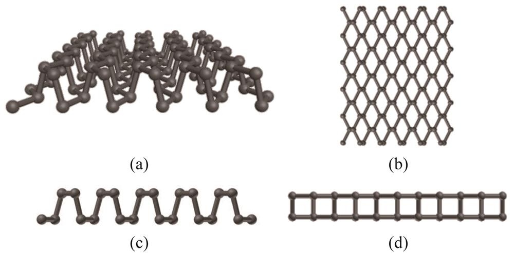
Fig. 1. Schematic diagram of phosphorene structure (a)3D phosphorene structure, (b)X-Y plane 2D phosphorene structure, (c)armchair direction, (d)zigzag direction
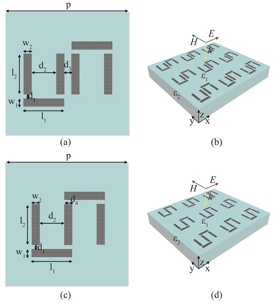
Fig. 2. Schematic diagram of structure (a)Cascaded π-structure 2D, (b)3D array, (c)compact π-structure 2D, (d)3D
Fig. 3. Transmission spectra under different structures Note: The system is illuminated normally by x-polarization plane wave and the geometric parameters are chosen as: l1 = l2 = 50 nm, w1 = w2 = 10 nm, d1 = 10 nm, d2 = 30 nm, the thickness of phosphorene is 10 nm, p = 220 nm, ɛ1 = ɛ2 =1; (a) and (b) are transmission spectra in x direction and y direction respectively; (c) shows the electric field distribution of A(5.42 μm), B(5.47 μm), C(5.48 μm) and D(5.56 μm) in fig. 3(a); (d) shows the electric field distribution of A(14.20 μm), B(14.50 μm), C(14.96 μm) and D(14.56 μm) in Figure 3(b); The electric field distribution diagram is observed in the x-y plane, and the unit is V/m.
Fig. 4. Transmission spectrua under π-cascade structure of phosphorene, Note: (a) and (b) indicate the transmission spectra when d3 is 10 nm, 20 nm, 30nm and 40 nm, respectively. The system is illuminated normally by x-polarization plane wave and the geometric parameters are chosen as: l1 = l2 = 50 nm, w1 = w2 = 10 nm, d1 = 10 nm, d2 = 30 nm, the thickness of phosphorene is 10 nm, p = 220 nm, ɛ1 = ɛ2 =1; (a) and (b) are transmission spectra in x direction and y direction respectively; (c) shows the electric field distribution of A(5.44 μm), B(5.46 μm), C(5.47 μm), D(5.48 μm), E(5.00 μm) and F(5.10 μm) in Fig. 4(a); (d) shows the electric field distribution of A(14.44 μm), B(14.47 μm), C(14.51 μm), D(14.56 μm), E(13.06 μm) and F(13.33 μm) in Fig. 4(b); The electric field distribution diagram is observed in the x-y plane, and the unit is V/m.
Fig. 5. Transmission spectra under compact π-structure of phosphorene Note: (a) and (b) indicate the transmission spectra when d4 is 0 nm, 5nm, 10 nm and 20 nm, respectively.The system is illuminated normally by x-polarization plane wave and the geometric parameters are chosen as: l1 = l2 = 50 nm, w1 = w2 = 10 nm, d1 = 10 nm, d2 = 30 nm, the thickness of phosphorene is 10 nm, p = 220 nm, ɛ1 = ɛ2 =1; (a) and (b) are transmission spectra in x direction and y direction respectively; (c) shows the electric field distribution of A(5.35 μm), B(5.31 μm), C(5.44 μm), D(5.51 μm), E(4.85 μm) and F(5.88 μm) in fig. 5(a); (d) shows the electric field distribution of A(14.23 μm), B(13.84 μm), C(14.62 μm), D(14.68 μm), E(12.96 μm) and F(15.68 μm) in Figure 5(b); The electric field distribution diagram is observed in the x-y plane, and the unit is V/m.
Fig. 6. Relationship between Fermi level and the position of transparent window under compact compact π-structure of phosphorene (a) the X direction, (b) the Y direction
Fig. 7. Relationship between incident light with different polarization angles and transmission under compact π-structure of phosphorene (a) is in the X direction, (b) is in the Y direction
|
Table 1. Physical parameters and their sources
| ||||||||||||||||||||||||
Table 2. Half width under different structures

Set citation alerts for the article
Please enter your email address
© Copyright 2018-2021 | Chinese Laser Press. All Rights Reserved 沪ICP备15018463号-20