• Journal of Semiconductors
  • Vol. 42, Issue 4, 041307 (2021)
Songtao Liu1 and Akhilesh Khope2
Author Affiliations
  • 1Ayar Labs, 3351 Olcott St, Santa Clara, CA 95054, USA
  • 2Microsoft Corporation, One Microsoft Way, Redmond, Washington, 98052, USA
  • show less
    DOI: 10.1088/1674-4926/42/4/041307 Cite this Article
    Songtao Liu, Akhilesh Khope. Latest advances in high-performance light sources and optical amplifiers on silicon[J]. Journal of Semiconductors, 2021, 42(4): 041307 Copy Citation Text show less

    Abstract

    Efficient light generation and amplification has long been missing on the silicon platform due to its well-known indirect bandgap nature. Driven by the size, weight, power and cost (SWaP-C) requirements, the desire to fully realize integrated silicon electronic and photonic integrated circuits has greatly pushed the effort of realizing high performance on-chip lasers and amplifiers moving forward. Several approaches have been proposed and demonstrated to address this issue. In this paper, a brief overview of recent progress of the high-performance lasers and amplifiers on Si based on different technology is presented. Representative device demonstrations, including ultra-narrow linewidth III–V/Si lasers, fully integrated III–V/Si/Si3N4 lasers, high-channel count mode locked quantum dot (QD) lasers, and high gain QD amplifiers will be covered.

    1. Introduction

    Driven by the exponential growth of the big data from the internet of things (IoT), 5G, high-performance computing, data center interconnects, and silicon photonics (SiP) has gained tremendous growth as it has the ability to address the high bandwidth and energy efficiency requirements since its first debut back in the 1980s[1-4]. Starting from the optimization of individual devices like low-loss waveguides, directional couplers, polarization rotators and modulators, the road to large-scale integration for SiP has begun. By leveraging the mature complementary metal–oxide–semiconductor (CMOS) technology, the monolithic integration density of SiP has reached up to 8192 individually addressed elements[5], far exceeding that of the state-of-the-art native substrate-based designs, which makes it an appealing host material for different applications, as shown in Fig. 1(a)[6]. It is forecasted that by 2025, the adoption of the SiP will reach an inflection point, where the share of SiP-based products will increase from 14% in 2018–2019 to 45% by 2025[7]. The most frequently used silicon-on-insulator (SOI) platform is particularly suited for the standard O- and C-communication bands. Although various designs based on the SOI platform have been demonstrated, the last piece of the puzzle — an efficient photon generation method — remain a challenge due to the indirect bandgap nature of silicon [8].

    (Color online) (a) Evolution of photonic integration in terms of the number of devices in a single PIC. Silicon photonic integration (red circle) represents the “passive” integration without an on-chip laser solution; InP integration (blue squares) and heterogeneous silicon integration (green triangle) are solutions with on-chip lasers[6]. (b) Schematic of the heterogeneous platform commercialized by Intel[10].

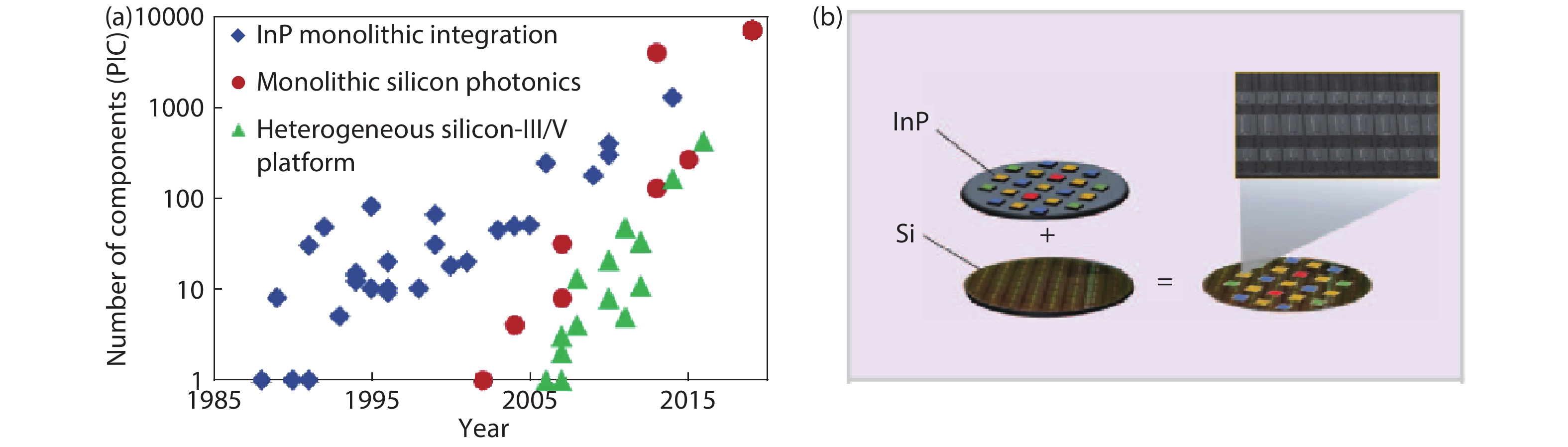
    Figure 1.(Color online) (a) Evolution of photonic integration in terms of the number of devices in a single PIC. Silicon photonic integration (red circle) represents the “passive” integration without an on-chip laser solution; InP integration (blue squares) and heterogeneous silicon integration (green triangle) are solutions with on-chip lasers[6]. (b) Schematic of the heterogeneous platform commercialized by Intel[10].

    Many approaches have been proposed in the past few decades, including Raman and Brillouin gain, rare-earth-ion implantation or combining the best of both worlds by heterogeneous integration or direct growth III–V on Si. Among those demonstrations, the most successful and prevalent approach at present is the heterogeneous integration scheme, where III–V material is bonded onto a pre-patterned Si wafer and then being processed together using standard lithography tools as shown in Fig. 1(b). Starting from the University of California, Santa Barbara (UCSB), in 2006[9], heterogeneously integrated lasers with different configurations and high gain amplifiers have been developed and presented with comparable performance to that of native lasers. Industrial implementations eventually evolved this scheme into mature commercial products that are being shipped in volume to fulfill the explosive growth of various applications with the need for size, weight, power and cost (SWaP-C) requirements[10]. Direct growth of III/V material on silicon, as an emerging technology, represents another direction of integration, which could potentially lead to the lowest chip cost ($/mm2) by growing, processing, testing, and packaging with commercially available 300 mm Si substrates[11]. Unlike heterogeneous integration, where lasers are integrated within Si photonic integrated circuits (PICs), most epitaxial research efforts are carried out in academia that have focused on optimizing discrete devices. The lattice constant mismatch and thermal expansion coefficient mismatch between III/V and Si need to be properly handled, which could result in a large dislocation density, causing device short lifetime and eventually failure[12].

    In this paper, we will review recent progresses on, non-exhaustively, novel light sources and amplifiers on Si based on the two most popular strategies that have been proposed and studied. Section 2 will focus on the narrow linewidth laser-based heterogeneous integration methodology, where a low-loss Si/SiN waveguide provided by the platform can be fully leveraged to improve the optical linewidth. By incorporating the low-loss waveguide as well as high-Q rings inside the cavity, a monolithically integrated semiconductor laser intrinsic linewidth below 200 Hz can be obtained, which is far exceeding the capability of native substrate-based lasers. Section 3 will discuss the potential and benefits provided by the direct epitaxial growth platform, where light sources and optical amplifiers can fully take advantage of the quantum dot (QD) material property. High channel count mode locked lasers (MLLs) and high gain amplifiers will be discussed in more detail. In the final section, we summarize and give a future outlook for this hot research field.

    2. Heterogeneously integrated lasers on Si

    The strong desire to integrate lasers within large-scale Si photonic integrated circuits (PICs) has pushed the research effort extensively in both academia and industry within the past several decades. Although Si Raman lasers[13], Ge-on-Si lasers[14] has been proposed and demonstrated, their inefficiency and complexity makes them the least appealing for massive production or integration within a Si PIC. Flip-chip bonding or butt coupling of a known-good III–V laser technique is currently widely adopted by the industry. However, the tight alignment requirement and the expensive packaging make them unsustainable for high-volume manufacturing (HVM). In order to address the bottleneck for the HVM, wafer bonding technology has been widely studied in the past decade, where the two main streams are O2 plasma-assisted direct wafer bonding and adhesive bonding using polymers[15]. In the fabrication process, a large piece of III–V known-good-die will be bonded and processed on a prepatterned 300 mm SOI wafer, where waveguides and other components are already defined by using standard CMOS-compatible processes. By defining the aligning markers directly on the SOI wafer, the alignment precision of III–V to Si will be much relaxed. High yield and HVM will be also obtained by leveraging advanced lithography and processing tools. Various laser demonstrations have been reported, including Fabry–Perot (FP) lasers[9], mode-locked lasers[16, 17], high-speed distributed feedback (DFB) lasers[18], micro-disk/ring lasers[19], widely tunable single wavelength lasers[20], and multi-wavelength lasers[21], etc. Large-scale integration designs containing more than 10 s of active component have also been shown[22]. Industrial implementations (Intel, Juniper, HPE etc) eventually evolved this scheme into mature commercial products that are being shipped in volume to fulfill the explosive growth of various applications with the need for size, weight, power and cost (SWaP-C) requirements[10]. Several good review papers on the technical details of different bonding processes and device performances can be found elsewhere[6, 23, 15].

    Future application scenarios, like coherent communications, on-chip optical sensing, laser gyroscopes, light detection and ranging (LiDAR) systems or precision metrology and timing would require further improvement on the laser performances with an emphasis on relative intensity noise (RIN) and frequency noise (optical linewidth)[24]. Traditionally, monolithically integrated semiconductor laser linewidth is on the order of MHz range with a few novel designs reaching sub-MHz linewidth range. The main dominant noise source comes from the amplified spontaneous emission (ASE) noise, which will contribute in both a direct and indirect way[25]. This leads to a modified Schawlow–Townes–Henry linewidth equation:

     (1)

    where Γ is the optical confinement factor, is the spontaneous emission rate that couples into the laser mode, is the photon density stored in the laser cavity and is the linewidth enhancement factor, which manifests the relationship between the imaginary and real parts of the refractive index. The linewidth optimization strategy will then become straightforwardly to be reducing the confinement factor and linewidth enhancement factor, increasing the photon lifetime within the laser cavity, etc. In the heterogeneous method, the optical mode expands in both the III–V region and the Si waveguide beneath. By changing the width of the Si waveguide, the mode confinement in the quantum well (QW) region can be easily controlled[26]. Because the loss in silicon is typically much lower than that of III–V cladding, a high-Q cavity can thus be easily obtained, which leads to low noise operation[27]. Extending the total cavity length by a low loss Si or Si3N4 waveguide could also be a choice[24]. Recent developments on ultra-low loss silicon waveguide has demonstrated 4 dB/m propagation loss performance[28]. This number can be even lower with the silicon nitride waveguide system[29]. This could help further improve the laser noise performance, making on-chip sub-kilohertz narrow linewidth lasers a reality.

    2.1. Ultra-narrow linewidth III–V/Si lasers

    Since the laser optical linewidth is fundamentally limited by the ASE noise, the first step to lower the optical linewidth is to decrease the ratio of the ASE noise that is coupled to the oscillating mode inside the laser cavity. By leveraging the heterogeneous silicon laser platform, Santis et al.[27] has successfully demonstrated the concept of improving the light coherence by separating the photon resonator and lossy active medium as shown in Fig. 2. By carefully engineering the high-Q silicon resonator, which is fashioned from a silicon waveguide patterned with a 1D grating [Fig. 2(c)], the resonator Q as high as 1.1 × 10⁶ has been shown. In this demonstration, even with a confinement factor as high as 15%, the laser exhibits a linewidth as low as 18 kHz. By further decreasing the Γ down to 1.5% in III–V and to only 0.2% in QW region, the measured optical Lorentzian linewidth is as low as 1 kHz[30], which is determined by the FM discriminator method quoting the white-noise limit, as shown in Fig. 2(d).

    (Color online) High-Q heterogeneous laser device schematics (not to scale). (a) Two-dimensional cross-section of the heterogeneous platform, with superimposed optical transverse mode profile. (b) Perspective view of a high-Q heterogeneous laser. (c) Perspective view of the high-Q silicon resonator[27]. (d) Frequency noise spectral density for three high-Q heterogeneous lasers (with different spacer thickness) and control laser[30].

    Figure 2.(Color online) High-Q heterogeneous laser device schematics (not to scale). (a) Two-dimensional cross-section of the heterogeneous platform, with superimposed optical transverse mode profile. (b) Perspective view of a high-Q heterogeneous laser. (c) Perspective view of the high-Q silicon resonator[27]. (d) Frequency noise spectral density for three high-Q heterogeneous lasers (with different spacer thickness) and control laser[30].

    A further improvement in both optical linewidth and output power could be obtained by incorporating a low loss Si external cavity. In order to keep the single mode operation, an on-chip filter with ultra-narrow full width half maximum (FWHM) bandwidth is needed. Recently Huang et al.[31] has demonstrated a fully integrated extended distributed Bragg reflector (DBR) laser. By designing the as low as 0.375, the overall FWHM bandwidth of the grating is only 2.9 GHz, which is narrow enough to pick out a single longitudinal cavity mode of the laser. Combining with the ultralow-loss silicon waveguide (0.16 dB/cm), 1 kHz optical linewidth and over 37 mW output power has been reported. This linewidth can be further enhanced by adding a high-Q ring inside the cavity, which would further reduce the linewidth to 500 Hz. Widely tunable single wavelength lasers with an ultralow noise laser operation could be obtained by designing a multi-ring mirror, as illustrated in Fig. 3(a), where multiple ring resonators are cascaded within a loop mirror. By carefully choosing the radius of different rings, a wide Vernier free spectral range and high passive side mode suppression ratio (SMSR >10 dB) across the whole span can be achieved. The benefits of incorporating rings inside the cavity are twofold: one is the cavity length enhancement, which can increase the photon lifetime due to effective cavity length lengthened and the second is the detuned loading effect, which can provide the negative optical feedback by slight detuning from the ring (resonator) resonance [32]. This could contribute to a further linewidth reduction. Tran et al.[24] has shown by utilizing four ring resonators, a tuning range of 120 nm from 1484 to 1604 nm and a Lorentzian linewidth of 140 Hz from a single laser can be obtained, which are records for both the tuning range and linewidth for single-chip fully integrated lasers ever reported (Fig. 3). An O-band laser with a 47 nm tuning range and a Lorentzian linewidth of 5.3 kHz leveraging a two-ring design is also reported[33].

    (Color online) (a) High-Q widely tunable heterogeneous quad-ring tunable laser device schematics (not to scale). (b) Coarse tuning spectra showing the tuning range of 120 nm. (c) Frequency noise spectrum of the fabricated quad-ring mirror laser. A white noise level of 45 Hz2/Hz is drawn[24].

    Figure 3.(Color online) (a) High-Q widely tunable heterogeneous quad-ring tunable laser device schematics (not to scale). (b) Coarse tuning spectra showing the tuning range of 120 nm. (c) Frequency noise spectrum of the fabricated quad-ring mirror laser. A white noise level of 45 Hz2/Hz is drawn[24].

    2.2. Fully integrated III–V/Si/SiN lasers

    A recent study has suggested that for high-Q Si resonators (Q > 10 6, radius ~ 100 µm), the nonlinear loss will start to dominate the total loss at even a relatively low power level (a few milliwatts in the bus waveguide)[34]. This is due to the two-photon absorption (TPA) and free carrier absorption (FCA) effect as Si has a relatively large TPA coefficient (βTPA = 5 × 10⁻¹² m/W at 1.55 µm). Although the previously mentioned high-Q ring resonators have helped to obtain the record narrow-linewidth laser performance, and the large waveguide cross-sections and large ring radius mitigate the nonlinear loss due to the decreased power intensity within the rings, the output power performance of those lasers, however, will still be limited within a few milliwatts level. Silicon nitride (Si3N4) waveguide platform, on the other hand, has negligible two photon absorption and free carrier generation due to its wide bandgap, which holds a great potential in achieving a high-power heterogeneously integrated narrow-linewidth tunable laser[35].

    The difficulty to realize an efficient III–V/Si3N4 laser lies in the large refractive index difference between those two materials (∆n ~ 1.3−1.5). Even extreme tapering of the thick III–V epitaxial layer is unable to facilitate efficient mode coupling between them within a III–V/Si3N4 structure. Chao et al.[36] has proposed a multilayer heterogeneous integration scheme that employs multiple mode transitions: the mode in the III–V/Si hybrid waveguide area will transition to a Si waveguide first and then through a Si/Si3N4 taper transitioning to the Si3N4 waveguide. Figs. 4(a) and 4(b) shows the schematic diagram of the laser design and the detailed taper design for efficient light coupling. A dual-level Si taper with a length of 200 μm is used to adiabatically couple the Si waveguide fundamental transverse electric (TE) mode to the Si3N4 waveguide fundamental TE mode through the hybridized Si/Si3N4 fundamental TE mode in the taper area. The monolithically integrated III–V/Si/SiN laser shows a lasing threshold of 75 mA with a peak on-chip output power over 0.5 mW for 320 mA gain current. The lasing wavelength centers around 1550 nm with the lowest obtained white-noise-limited frequency noise level down to 1300 Hz2/Hz, giving a Lorentzian linewidth of 4 kHz [Fig. 4(c)]. This value is mainly limited by a relatively large waveguide propagation loss of 0.43 dB/cm due to a fab error, which can be further reduced to around 0.001–0.01 dB/cm range, leading to a much-improved laser linewidth. A similarly design has also been reported leveraging microtransfer printing, where a III/V-on-Si3N4 optical amplifier with a 13.7 dB on-chip gain and a III/V-on-Si3N4 ring laser have been shown[37]. Park et al. has also demonstrated the first heterogeneously integrated electrically pumped GaAs lasers and detectors coupled to SiN waveguides, where the laser works around 990 nm with a threshold around 180 mA[38]. The wafer-scale process makes those designs appealing for many fields including nonlinear photonics, optical sensing, displays, quantum sensing and computing, etc.

    (Color online) (a) III–V/Si/Si3N4 laser schematic diagram. (b) Si–Si3N4 taper as well as the simulated mode profile. (c) Single-mode optical spectrum with gain current of 160 mA. The inset shows measured normalized reflection spectra of the Si3N4 spiral grating[36].

    Figure 4.(Color online) (a) III–V/Si/Si3N4 laser schematic diagram. (b) Si–Si3N4 taper as well as the simulated mode profile. (c) Single-mode optical spectrum with gain current of 160 mA. The inset shows measured normalized reflection spectra of the Si3N4 spiral grating[36].

    2.3. Heterogeneous integrated III–V/Si optical amplifiers

    As the silicon PICs continue to scale to larger, more complex configurations, one of the biggest issues is the accumulated insertion loss from those passive switches, waveguide crossings, and couplers, which would put high power requirements on the light source and cause problems with loss due to two photon absorption[39]. In-line semiconductor optical amplifiers (SOAs) are a natural solution to help alleviate the requirement on the light source side, compensate for the path loss to maintain channel equalization and signal preamplification. Most of the SOA on silicon demonstrations all employ the wafer bonding technique, with the epi layer the same as the gain material in the lasers. Thus, the optical gain bandwidth of the SOA should be as large as the laser’s gain material, which offers great design simplicity.

    In terms of the SOA design, several figures of merit include the small signal gain factor , which is the ratio of the output power to the input power, the output saturation power , which is the out power level at which the gain has been reduced to half of its unsaturated value, and the noise figure (NF), which is the degradation in optical signal-to-noise ratio (OSNR) after amplification can be engineered to achieve the best amplification performance[40]. The small signal gain factor can be increased by enlarging the confinement factor as well as to lengthen the SOA length, but if this is too long the SOA length will easily lead to gain saturation due to the presence of strong ASE intensity in long devices[41]. On the other hand, reducing the confinement factor leads to the increase of the output saturation power as well as reduction of the NF. However, the will be reduced correspondingly. Increasing the modal area is another way to increase the , however, the coupling will be challenging because of the large mode mismatch between the waveguide and fiber.

    Similar to the lasers bonded on Si, the SOAs can be realized with the same epi design and fabrication process[42]. To prevent the devices from lasing, the SOAs generally are designed with angled and anti-reflection (AR) coated polished heterogeneous facets. By varying the Si waveguide width as well as the III–V multi quantum well layer, control of the confinement factor can be easily achieved, which determines the gain and saturation output power. The first SOA on Si reported in 2007 shows a maximum on-chip gain of 13 dB and a 3-dB output saturation power of 11 dBm by direct wafer bonding method[42]. Further improvements can be obtained by the optimization of thermal and electrical properties of the device, which is showed in Ref. [43] where small signal gain of 25.5 dB and saturation output power of 16.25 dBm are shown. The highest wall plug efficiency of 12.1% is also reported by improving the electrical property of the amplifier with a low resistance[44]. A more recent result shows a 27 dB on-chip small-signal gain, 17.24 dBm saturation power for heterogeneously integrated Si/III–V SOA by utilizing the divinylsiloxane-bis-benzocyclobutene (DVS-BCB) adhesive die-to-wafer bonding method, where an optical confinement of 0.7 % per well is adopted to increase the [45].

    3. Monolithically integrated QD lasers and amplifiers on Si

    Over the past five years, there has been tremendous progress in this area to directly grow III–Vs on Si[46-50]. Although the lattice constant mismatch and thermal expansion coefficient mismatch still remain, the adoption of the QD material makes the monolithic integration of the gain section on Si a reality. Unlike the QW material, the zero-dimensional, particle-in-a-box-like quantum confined QD structure enables strong three-dimensional carrier confinement, which makes the QD less sensitive to the threading dislocations (TDs) originating from the lattice and thermal mismatch[51]. A direct comparison of QD and QW performance on identical III–V/Si templates has been shown in Ref. [52], where the ability for QDs to tolerate residual dislocations has been confirmed. With a substrate template TD density of 7 × 106 cm−2, QD material grown on the Si substrate shows a nearly identical room temperature photoluminescence intensity when compared to that of the QD grown on native substrate, as shown in Fig. 5[47]. The adoption of the QD gain material on Si has other benefits that originate from the unique material properties of the QD. The inhomogeneously broadened gain would translate to a wide working bandwidth (benefits for widely tunable single wavelength lasers, mode locked lasers, optical amplifiers, etc); the low threshold current density, low internal loss and low confinement factor would establish a low noise operation; the high temperature stability would lead to uncooled operation; and the ultrafast absorption recovery response would make the laser suitable to generate sub-picosecond pulses. All of these have suggested the promising potential of realizing high-performance light sources on Si.

    (Color online) (a) Schematic illustration of the typical epitaxial structure used for lasers and amplifiers including one period of the p-modulation doped active region and the III–V/Si buffer including defect filter layers and thermal cycle annealing (TCA) to reduce dislocation densities. (b) As-grown photoluminescence spectra for quantum dot lasers on GaAs and Si substrates[47].

    Figure 5.(Color online) (a) Schematic illustration of the typical epitaxial structure used for lasers and amplifiers including one period of the p-modulation doped active region and the III–V/Si buffer including defect filter layers and thermal cycle annealing (TCA) to reduce dislocation densities. (b) As-grown photoluminescence spectra for quantum dot lasers on GaAs and Si substrates[47].

    Previous reports of direct growth methods on Si are mainly based on the 4°–6° offcut Si substrate in order to suppress antiphase domains, which comes from the combination of polar and non-polar bonds. In 2011, University College London (UCL) reported the first electrically pumped 1.3 μm InAs QD laser that was grown directly on a Si (001) substrate with a 4° off-cut[53]. Various configurations have then been published with decent laser performance shown. To further leverage the CMOS advantage, recent research focus has transitioned from the offcut Si substrate to on-axis (001) silicon substrates. UCSB in 2017 has demonstrated the first electrically pumped continuous-wave III–V QD FP laser operating at room temperature and above, which was epitaxially grown on on-axis GaP/silicon substrates without offcut or germanium buffers[54]. A 2.3 μm GaAs buffer layer was then grown on the GaP/Si template in a solid-source molecular beam epitaxy (MBE). A thermal annealing cycle was employed after the growth of the GaAs buffer to facilitate dislocation annihilation. In the same year, UCL has also reported the FP lasers that were monolithically grown on the on-axis Si (001) substrates but without any intermediate buffer layers[55], where the laser operates at room-temperature lasing at ~1.3 µm with a threshold current density of 425 A/cm2 and single facet output power of 43 mW. Since then, various laser designs have been reported, including sub-milliamp threshold micro ring lasers[56], microdisk lasers[57], tunable single wavelength lasers[58], high-gain and wide amplification bandwidth semiconductor optical amplifiers[59], QD mode locked lasers (MLLs)[60, 61], monolithic QD distributed feedback laser arrays[62, 63], and low dark current photodiodes[64], etc. FP lasers monolithically grown on a silicon-on-insulator (SOI) substrate has also been reported, which shows great promise towards fully integrated Si PICs[65]. Recent research has shown that with a ~7 × 106 cm–2 threading dislocation density, laser lifetime can exceeds more than a million an hour based on the CMOS-compatible on-axis (001) Si substrate[51]. It is paramount that uniform arrays of QDs exhibits a low linewidth enhancement factor[66, 67], which leads to an insensitive operation to reflections, even with 90% of the output light being reflected back into the cavity[68]. Technical details of direct growth technology and reviews of previous laser demonstrations can be found in Refs. [47, 52]. The demonstrated performance of the QD laser library indicates a huge commercialization possibility, which will make them competitive components for future large-scale silicon PICs when epitaxial growth becomes mature.

    3.1. Mode locked QD lasers

    MLLs can generate wide coherent combs, which consist of equally spaced optical lines in the frequency domain[69, 70]. Semiconductor-based MLLs take advantage of small footprint, high wall-plug efficiency, low fabrication cost, mass producibility, and high integration capability, which has regained new attention as it has been recognized as a promising light source for co-packaged optics (CPO), which adopts the wavelength division multiplexing (WDM) architecture to address the power and bandwidth requirements for the mega data centers[39]. It has been demonstrated that semiconductor MLLs can be used as comb sources for WDM systems to increase the transmission capacity[71]. MLLs can also be used as transmitters in WDM switching applications, where a WDM switch can either be single or multi-wavelength selective[72, 73]. By leveraging the QD on the Si platform, low noise and high channel count MLLs can be realized. UCSB has demonstrated the first MLLs that are directly grown on the CMOS compatible Si (001) substrate with different channel spacings within the past two years. By changing the cavity length as well as designing the saturable absorber (SA) positions, 9 GHz[74], 20 GHz[60], 31 GHz[75] and 100 GHz[76] channel spacings with different channel counts have been shown. Fig. 6(a) shows a classical two-section MLL with one SA section located at the end of the facet and the rest is the gain section, which are electrically isolated from each other by a second dry etch process[60]. Corresponding optical spectrum is shown in Fig. 6(b), showing a flat top shape, which is typical for QD-based devices. Low relative intensity noise (RIN) is another advantage demonstrated by the QD-based MLL. The integrated average RIN values for the whole spectrum and a single channel are −152 and −133 dB/Hz (range from 10 MHz to 10 GHz), respectively as shown in Fig. 6(c). Meanwhile, benefiting from the low internal loss and low confinement factor property, low noise operation has also been shown with a 400 Hz RF 3 dB linewidth, which is the narrowest value ever reported from a high speed passively mode locked semiconductor laser[77]. System level B2B and 5 km transmission with a Nyquist four-level pulse amplitude modulation format has been shown in Fig. 6(d). By leveraging 64 channels, a 4.1 terabits per second total transmission bandwidth has been achieved[78].

    (Color online) (a) Schematic diagram of the 20 GHz quantum dot mode-locked laser on silicon (not to scale). (b) Optical spectrum and corresponding optical linewidth of each mode within 10 dB. (c) Relative intensity noise of the whole O-band spectrum and certain filtered individual wavelength channels. (d) BER performance of the PAM-4 signal with different comb lines[60].

    Figure 6.(Color online) (a) Schematic diagram of the 20 GHz quantum dot mode-locked laser on silicon (not to scale). (b) Optical spectrum and corresponding optical linewidth of each mode within 10 dB. (c) Relative intensity noise of the whole O-band spectrum and certain filtered individual wavelength channels. (d) BER performance of the PAM-4 signal with different comb lines[60].

    Typical mode locked lasers utilize a two-section structure, where the laser cavity is separated into two sections by an electrical isolation, one gain section for mode amplification and one saturable absorber (SA) section for pulse formation. When in operation, the gain section will be forward current biased and the SA section will be reverse voltage biased. Due to the nonlinear absorption effect of the SA, a pulse will be formed. Recently, several interesting findings reveal that by using a single section gain structure based on the QD material, a pulse can also be formed inside the cavity[79-81]. UCSB has also shown this interesting phenomenon on the Si platform[75]. This is very appealing as the adoption of the SA section will introduce loss inside the cavity, which will decrease the output power as well as the wall plug efficiency. Currently, there is still some debate on whether one is seeing self-mode locking or unaccounted saturable absorption from, e.g., uneven current injection. Several theoretical papers have proposed that four-wave mixing (FWM) causes the locking of beat frequencies among lasing modes, which arises from nonlinearities in light-matter interactions within an inhomogeneously broadened distribution of QDs providing gain to a large number of lasing modes [82, 83]. More investigations are currently underway.

    3.2. High gain QD amplifiers

    In terms of SOA, QD material has shown multiple advantages compared to its bulk or QW counterparts[84]. The fast gain response makes it suitable to amplify high-speed signals without the pattern effect; the high temperature stability leads it to uncooled operation; the low threshold current density, low internal loss and low confinement factor establish it with low noise figure operation; the inhomogeneously broadened gain translates to a wide amplification bandwidth. QD-SOAs based on native substrates have shown > 25 dB on chip gain, > 20 dBm saturation output power, < 5 dB NF and 120 nm amplification bandwidth [84]. It is natural to transfer the QD SOA design to the QD direct growth Si platform developed at UCSB. In 2019, the first QD-SOA directly grown on the CMOS compatible Si substrate has been reported[59]. Due to the small gain per unit length, the SOA is designed to have a length of 5000 μm in order to obtain a large on-chip small signal gain. The device ridge width is also tapered monotonically from 5 to 11 μm to increase the modal area, which could lead to large saturation output power. The chip shows a maximum on-chip small signal gain of 39 dB, a minimum noise figure of 6.6 dB, saturation output power of 24 dBm, > 100 nm amplification bandwidth (gain > 20 dB) and wall plug efficiency of 20% ( Fig. 7). The introduction of p-modulation doping in the spacer layer further helps to improve the temperature performance. The SOA shows a larger than 20 dB gain in a 21 nm wavelength range at 70 °C. By leveraging this high-performance QD-SOA as a preamplifier in a filterless 60-Gbit/s NRZ transmission system, the receiver sensitivity has been enhanced over a wide wavelength range from 1280 nm to 1340 nm and temperature range from 20 to 60 °C. At least 15 dB photoreceiver sensitivity improvement with a minimum sensitivity of –25 dBm is demonstrated at 20 °C[85].

    (Color online) Si-based QD-SOA (a) on-chip gain (TE polarization) mapping as a function of on-chip input power and wavelength at 20 °C. (b) On-chip small signal gain as a function of wavelength. (c) On-chip output power as a function of on-chip input power. (d) Wall-plug efficiency as a function of on-chip input power[59]. (e) Bit error rate (BER) against the received optical power for the optical receiver (PD+TIA) with and without QD-SOA under 20 °C, eye diagrams of the receiver with and without QD-SOA are shown in the insets[85].

    Figure 7.(Color online) Si-based QD-SOA (a) on-chip gain (TE polarization) mapping as a function of on-chip input power and wavelength at 20 °C. (b) On-chip small signal gain as a function of wavelength. (c) On-chip output power as a function of on-chip input power. (d) Wall-plug efficiency as a function of on-chip input power[59]. (e) Bit error rate (BER) against the received optical power for the optical receiver (PD+TIA) with and without QD-SOA under 20 °C, eye diagrams of the receiver with and without QD-SOA are shown in the insets[85].

    4. Conclusions

    In this paper, latest progresses on high-performance light sources and amplifiers integrated on silicon based on the heterogeneous or direct growth method have been reviewed. Several detailed examples are given, including narrow linewidth lasers, mode-locked lasers and high gain amplifiers. In general, heterogeneous integration at present offers the greatest flexibility and scalability in terms of the PIC integration capability, where multiple III/V dies can be arbitrarily bonded at any position on a 300 mm silicon wafer. Commercialization is driving its maturity into the product level. Recent results on the hertz-level linewidth semiconductor lasers leveraging CMOS-ready ultra-high-Q microresonators[35] indicates a new direction for the monolithically integrated narrow linewidth lasers, where an ultra-low loss silicon nitride waveguide (0.045 dB/m) and self-injection locking technique are utilized, leading to a 3 Hz optical linewidth generation. The CMOS-ready silicon nitride waveguide platform also indicates the scalable production capability with high yield using foundry-based technologies. Meanwhile, as the direct growth technology gradually moves ahead (low threshold lasers, 1-million-hour-long lifetime, etc.), research interests would finally turn into exploring the ways to integrate QD lasers seamlessly with passive silicon waveguides. Although the thick buffer layer on the growth template would make the efficient coupling to the Si waveguide very challenging, several possible integration schemes have been proposed[86] and efforts toward that direction has started to show[87]. We hope that fully integrated large-scale silicon electronic and photonic integrated circuits with the lowest cost and highest functionality will eventually become a reality.

    Acknowledgements

    The authors would like to thank all the members of the UCSB Prof. John Bowers group for the material and useful discussions.

    References

    [1] A Rahim, T Spuesens, R Baets et al. Open-access silicon photonics: Current status and emerging initiatives. Proc IEEE, 106, 2313(2018).

    [2] T Pinguet, S Denton, S Gloeckner et al. High-volume manufacturing platform for silicon photonics. Proc IEEE, 106, 2281(2018).

    [3] X Chen, M M Milosevic, S Stanković et al. The emergence of silicon photonics as a flexible technology platform. Proc IEEE, 106, 2101(2018).

    [4] M Glick, N C Abrams, Q X Cheng et al. PINE: photonic integrated networked energy efficient datacenters (ENLITENED program). J Opt Commun Netw, 12, 443(2020).

    [5]

    [6] T Komljenovic, D N Huang, P Pintus et al. Photonic integrated circuits using heterogeneous integration on silicon. Proc IEEE, 106, 2246(2018).

    [7]

    [8] D Liang, J E Bowers. Recent progress in lasers on silicon. Nat Photonics, 4, 511(2010).

    [9] A W Fang, H Park, O Cohen et al. Electrically pumped hybrid AlGaInAs-silicon evanescent laser. Opt Express, 14, 9203(2006).

    [10] R Jones, P Doussiere, J B Driscoll et al. Heterogeneously integrated InP\/silicon photonics: Fabricating fully functional transceivers. IEEE Nanotechnol Mag, 13, 17(2019).

    [11] A Y Liu, J Bowers. Photonic integration with epitaxial III–V on silicon. IEEE J Sel Top Quantum Electron, 24, 6000412(2018).

    [12] J C Norman, D Jung, Y T Wan et al. Perspective: The future of quantum dot photonic integrated circuits. APL Photonics, 3, 030901(2018).

    [13] H S Rong, S B Xu, Y H Kuo et al. Low-threshold continuous-wave Raman silicon laser. Nat Photonics, 1, 232(2007).

    [14] J F Liu, X C Sun, R Camacho-Aguilera et al. Ge-on-Si laser operating at room temperature. Opt Lett, 35, 679(2010).

    [15] Z C Wang, A Abbasi, U Dave et al. Novel light source integration approaches for silicon photonics. Laser Photonics Rev, 11, 1700063(2017).

    [16] A W Fang, B R Koch, K G Gan et al. A racetrack mode-locked silicon evanescent laser. Opt Express, 16, 1393(2008).

    [17] Z C Wang, K van Gasse, V Moskalenko et al. A III-V-on-Si ultra-dense comb laser. Light: Sci Appl, 6, e16260(2017).

    [18] C Zhang, S Srinivasan, Y Tang et al. Low threshold and high speed short cavity distributed feedback hybrid silicon lasers. Opt Express, 22, 10202(2014).

    [19] D Liang, X Huang, G Kurczveil et al. Integrated finely tunable microring laser on silicon. Nat Photonics, 10, 719(2016).

    [20] T Komljenovic, S Srinivasan, E Norberg et al. Widely tunable narrow-linewidth monolithically integrated external-cavity semiconductor lasers. IEEE J Sel Top Quantum Electron, 21, 214(2015).

    [21] G Kurczveil, M J R Heck, J D Peters et al. An integrated hybrid silicon multiwavelength AWG laser. IEEE J Sel Top Quantum Electron, 17, 1521(2011).

    [22] C Zhang, S J Zhang, J D Peters et al. 8 × 8 × 40 Gbps fully integrated silicon photonic network on chip. Optica, 3, 785(2016).

    [23] G Roelkens, L Liu, D Liang et al. III-V/silicon photonics for on-chip and intra-chip optical interconnects. Laser Photonics Rev, 4, 751(2010).

    [24] M A Tran, D N Huang, J E Bowers. Tutorial on narrow linewidth tunable semiconductor lasers using Si/III-V heterogeneous integration. APL Photonics, 4, 111101(2019).

    [25] C Henry. Theory of the linewidth of semiconductor lasers. IEEE J Quantum Electron, 18, 259(1982).

    [26] M L Davenport, S T Liu, J E Bowers. Integrated heterogeneous silicon/III–V mode-locked lasers. Photon Res, 6, 468(2018).

    [27] C T Santis, S T Steger, Y Vilenchik et al. High-coherence semiconductor lasers based on integral high-Q resonators in hybrid Si/III-V platforms. Proc Natl Acad Sci USA, 111, 2879(2014).

    [28] M Tran, D N Huang, T Komljenovic et al. Ultra-low-loss silicon waveguides for heterogeneously integrated silicon/III-V photonics. Appl Sci, 8, 1139(2018).

    [29] J F Bauters, M J R Heck, D John et al. Ultra-low-loss high-aspect-ratio Si3N4 waveguides. Opt Express, 19, 3163(2011).

    [30]

    [31] D N Huang, M A Tran, J Guo et al. High-power sub-kHz linewidth lasers fully integrated on silicon. Optica, 6, 745(2019).

    [32] B Liu, A Shakouri, J E Bowers. Passive microring-resonator-coupled lasers. Appl Phys Lett, 79, 3561(2001).

    [33] A Malik, J Guo, M A Tran et al. Widely tunable, heterogeneously integrated quantum-dot O-band lasers on silicon. Photon Res, 8, 1551(2020).

    [34] C Xiang, W Jin, J Guo et al. Effects of nonlinear loss in high-Q Si ring resonators for narrow-linewidth III-V/Si heterogeneously integrated tunable lasers. Opt Express, 28, 19926(2020).

    [35]

    [36] C Xiang, W Jin, J Guo et al. Narrow-linewidth III-V/Si/Si3N4 laser using multilayer heterogeneous integration. Optica, 7, 20(2020).

    [37] C O de Beeck, B Haq, L Elsinger et al. Heterogeneous III-V on silicon nitride amplifiers and lasers via microtransfer printing. Optica, 7, 386(2020).

    [38] H Park, C Zhang, M A Tran et al. Heterogeneous silicon nitride photonics. Optica, 7, 336(2020).

    [39] Q X Cheng, M Bahadori, M Glick et al. Recent advances in optical technologies for data centers: A review. Optica, 5, 1354(2018).

    [40]

    [41] T W Berg, J Mork. Saturation and noise properties of quantum-dot optical amplifiers. IEEE J Quantum Electron, 40, 1527(2004).

    [42] H Park, A W Fang, O Cohen et al. A hybrid AlGaInAs–silicon evanescent amplifier. IEEE Photonics Technol Lett, 19, 230(2007).

    [43] M L Davenport, S Skendžić, N Volet et al. Heterogeneous silicon/III –V semiconductor optical amplifiers. IEEE J Sel Top Quantum Electron, 22, 78(2016).

    [44] S Cheung, Y Kawakita, K Shang et al. Highly efficient chip-scale III –V/silicon hybrid optical amplifiers. Opt Express, 23, 22431(2015).

    [45] K van Gasse, R J Wang, G Roelkens. 27 dB gain III–V-on-silicon semiconductor optical amplifier with > 17 dBm output power. Opt Express, 27, 293(2019).

    [46] S M Chen, W Li, J Wu et al. Electrically pumped continuous-wave III–V quantum dot lasers on silicon. Nat Photonics, 10, 307(2016).

    [47] J C Norman, D Jung, Z Y Zhang et al. A review of high-performance quantum dot lasers on silicon. IEEE J Quantum Electron, 55, 2000511(2019).

    [48] S J Pan, V Cao, M Y Liao et al. Recent progress in epitaxial growth of III –V quantum-dot lasers on silicon substrate. J Semicond, 40, 101302(2019).

    [49] B Shi, Y Han, Q Li et al. 1.55-μm lasers epitaxially grown on silicon. IEEE J Sel Top Quantum Electron, 25, 1900711(2019).

    [50] W Q Wei, Q Feng, Z H Wang et al. Perspective: optically-pumped III–V quantum dot microcavity lasers via CMOS compatible patterned Si (001) substrates. J Semicond, 40, 53(2019).

    [51] D Jung, Z Y Zhang, J Norman et al. Highly reliable low-threshold InAs quantum dot lasers on on-axis (001) Si with 87% injection efficiency. ACS Photonics, 5, 1094(2018).

    [52] A Y Liu, S Srinivasan, J Norman et al. Quantum dot lasers for silicon photonics. Photonics Res, 3, B1(2015).

    [53] T Wang, H Liu, A Lee et al. 1.3-μm InAs/GaAs quantum-dot lasers monolithically grown on Si substrates. Opt Express, 19, 11381(2011).

    [54] A Y Liu, J Peters, X Huang et al. Electrically pumped continuous-wave 13 μm quantum-dot lasers epitaxially grown on on-axis (001) GaP/Si. Opt Lett, 42, 338(2017).

    [55] S M Chen, M Y Liao, M C Tang et al. Electrically pumped continuous-wave 1.3 μm InAs/GaAs quantum dot lasers monolithically grown on on-axis Si (001) substrates. Opt Express, 25, 4632(2017).

    [56] Y T Wan, J Norman, Q Li et al. 13 μm submilliamp threshold quantum dot micro-lasers on Si. Optica, 4, 940(2017).

    [57] W Q Wei, J Y Zhang, J H Wang et al. Phosphorus-free 1.5 μm InAs quantum-dot microdisk lasers on metamorphic InGaAs/SOI platform. Opt Lett., 45, 2042(2020).

    [58] Y T Wan, S Zhang, J C Norman et al. Tunable quantum dot lasers grown directly on silicon. Optica, 6, 1394(2019).

    [59] S T Liu, J Norman, M Dumont et al. High-performance O-band quantum-dot semiconductor optical amplifiers directly grown on a CMOS compatible silicon substrate. ACS Photonics, 6, 2523(2019).

    [60] S T Liu, X R Wu, D Jung et al. High-channel-count 20 GHz passively mode-locked quantum dot laser directly grown on Si with 4.1 Tbit/s transmission capacity. Optica, 6, 128(2019).

    [61] Z Y Zhang, Z Y Zhang, J C Norman et al. Integrated dispersion compensated mode-locked quantum dot laser. Photon Res, 8, 1428(2020).

    [62] Y Wang, S M Chen, Y Yu et al. Monolithic quantum-dot distributed feedback laser array on silicon. Optica, 5, 528(2018).

    [63] Y T Wan, J C Norman, Y Y Tong et al. Quantum dot lasers: 1.3 μm quantum dot-distributed feedback lasers directly grown on (001) Si (laser photonics rev. 14(7)/2020). Laser Photonics Rev, 14, 2070042(2020).

    [64] B L Chen, Y T Wan, Z Y Xie et al. Low dark current high gain InAs quantum dot avalanche photodiodes monolithically grown on Si. ACS Photonics, 7, 528(2020).

    [65] W Q Wei, Q Feng, J J Guo et al. InAs/GaAs quantum dot narrow ridge lasers epitaxially grown on SOI substrates for silicon photonic integration. Opt Express, 28, 26555(2020).

    [66] Z Y Zhang, D Jung, J C Norman et al. Linewidth enhancement factor in InAs/GaAs quantum dot lasers and its implication in isolator-free and narrow linewidth applications. IEEE J Sel Top Quantum Electron, 25, 1900509(2019).

    [67] W W Chow, Z Y Zhang, J C Norman et al. On quantum-dot lasing at gain peak with linewidth enhancement factor αH = 0. APL Photonics, 5, 026101(2020).

    [68] H M Huang, J N Duan, D Jung et al. Analysis of the optical feedback dynamics in InAs/GaAs quantum dot lasers directly grown on silicon. J Opt Soc Am B, 35, 2780(2018).

    [69] M G Thompson, A R Rae, M Xia et al. InGaAs quantum-dot mode-locked laser diodes. IEEE J Sel Top Quantum Electron, 15, 661(2009).

    [70] S T Liu, H T Wang, M D Sun et al. AWG-based monolithic 4 × 12 GHz multichannel harmonically mode-locked laser. IEEE Photonics Technol Lett, 28, 241(2016).

    [71] J N Kemal, P Marin-Palomo, V Panapakkam et al. WDM transmission using quantum-dash mode-locked laser diodes as multi-wavelength source and local oscillator. 2017 Opt Fiber Commun Conf Exhib OFC, 1(2017).

    [72] A S P Khope, M Saeidi, R Yu et al. Multi-wavelength selective crossbar switch. Opt Express, 27, 5203(2019).

    [73] A S P Khope, S T Liu, Z Y Zhang et al. 2 λ switch. Opt Lett, 45, 5340(2020).

    [74] S T Liu, J C Norman, D Jung et al. Monolithic 9 GHz passively mode locked quantum dot lasers directly grown on on-axis (001) Si. Appl Phys Lett, 113, 041108(2018).

    [75] S Liu, D Jung, J C Norman et al. 490 fs pulse generation from passively mode-locked single section quantum dot laser directly grown on on-axis GaP/Si. Electron Lett, 54, 432(2018).

    [76] S T Liu, X R Wu, J Norman et al. 100 GHz colliding pulse mode locked quantum dot lasers directly grown on Si for WDM application. Conference on Lasers and Electro-Optics, ATu3P-5(2019).

    [77] D Auth, S Liu, J Norman et al. Passively mode-locked semiconductor quantum dot on silicon laser with 400 Hz RF line width. Opt Express, 27, 27256(2019).

    [78] X R Wu, S T Liu, D Jung et al. Terabit interconnects with a 20-GHz O-band passively mode locked quantum dot laser grown directly on silicon. Optical Fiber Communication Conference (OFC), W2A-3(2019).

    [79] Z G Lu, J R Liu, S Raymond et al. 312-fs pulse generation from a passive C-band InAs/InP quantum dot mode-locked laser. Opt Express, 16, 10835(2008).

    [80] F Gao, S Luo, H M Ji et al. Single-section mode-locked 1.55-μm InAs/InP quantum dot lasers grown by MOVPE. Opt Commun, 370, 18(2016).

    [81] R Rosales, S G Murdoch, R T Watts et al. High performance mode locking characteristics of single section quantum dash lasers. Opt Express, 20, 8649(2012).

    [82] W W Chow, S T Liu, Z Y Zhang et al. Multimode description of self-mode locking in a single-section quantum-dot laser. Opt Express, 28, 5317(2020).

    [83] P Bardella, L L Columbo, M Gioannini. Self-generation of optical frequency comb in single section quantum dot Fabry-Perot lasers: A theoretical study. Opt Express, OE, 25, 26234(2017).

    [84] T Akiyama, M Sugawara, Y Arakawa. Quantum-dot semiconductor optical amplifiers. Proc IEEE, 95, 1757(2007).

    [85] S T Liu, Y Y Tong, J Norman et al. High efficiency, high gain and high saturation output power quantum dot SOAs grown on Si and applications. Optical Fiber Communication Conference (OFC), 1(2020).

    [86] J E Bowers, A Gossard, D Jung et al. Quantum dot photonic integrated circuits on silicon. Conference on Lasers and Electro-Optics, 1(2018).

    [87] Y Han, Z Yan, W K Ng et al. Bufferless 1.5 μm III-V lasers grown on Si-photonics 220 nm silicon-on-insulator platforms. Optica, 7, 148(2020).

    Songtao Liu, Akhilesh Khope. Latest advances in high-performance light sources and optical amplifiers on silicon[J]. Journal of Semiconductors, 2021, 42(4): 041307
    Download Citation