• Photonics Research
  • Vol. 10, Issue 8, 1964 (2022)
Xiaoshuai An1、2, Hongying Yang1, Yumeng Luo1, Zhiqin Chu2、3、6、*, and Kwai Hei Li1、4、5、7、*
Author Affiliations
  • 1School of Microelectronics, Southern University of Science and Technology, Shenzhen 518055, China
  • 2Department of Electrical and Electronic Engineering, The University of Hong Kong, Hong Kong, China
  • 3School of Biomedical Sciences, The University of Hong Kong, Hong Kong, China
  • 4Engineering Research Center of Integrated Circuits for Next-Generation Communications, Ministry of Education, Southern University of Science and Technology, Shenzhen 518055, China
  • 5Engineering Research Center of Three Dimensional Integration in Guangdong Province, Southern University of Science and Technology, Shenzhen 518055, China
  • 6e-mail: zqchu@eee.hku.hk
  • 7e-mail: khli@sustech.edu.cn
  • show less
    DOI: 10.1364/PRJ.462933 Cite this Article Set citation alerts
    Xiaoshuai An, Hongying Yang, Yumeng Luo, Zhiqin Chu, Kwai Hei Li. Ultrafast miniaturized GaN-based optoelectronic proximity sensor[J]. Photonics Research, 2022, 10(8): 1964 Copy Citation Text show less
    (a) Schematic diagrams showing the fabrication process flow of the GaN chip. (b) Optical image of the packaged chip; inset shows the enlarged image of the chip. Scale bar is 500 μm. (c) Schematic diagram depicting the operating principle of the proximity sensor.
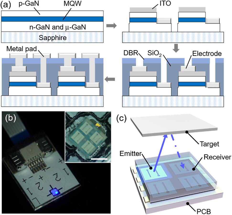
    Fig. 1. (a) Schematic diagrams showing the fabrication process flow of the GaN chip. (b) Optical image of the packaged chip; inset shows the enlarged image of the chip. Scale bar is 500 μm. (c) Schematic diagram depicting the operating principle of the proximity sensor.
    (a) I-V characteristic of the on-chip unit as an emitter. Inset shows the light output intensity as a function of injection current. (b) Emission spectrum of the emitter operating at 10 mA and reflectance plot of the DBR measured at normal incidence; (c) I-V characteristic of the on-chip unit as a receiver when the emitter operates at different currents; (d) I-V characteristic of the receiver measured at reverse bias voltages of up to −20 V; (e) plot of photocurrent of the receiver versus driving current of the emitter; (f) photocurrent as a function of the distance of the sensor from the films with varying reflectance; inset shows photocurrent change versus the distance of the sensor from the films on a logarithmic scale.
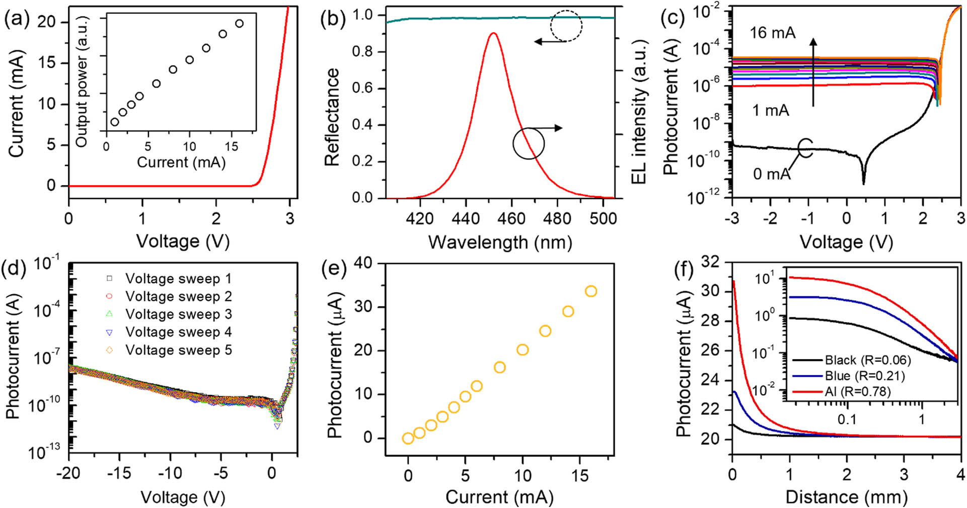
    Fig. 2. (a) I-V characteristic of the on-chip unit as an emitter. Inset shows the light output intensity as a function of injection current. (b) Emission spectrum of the emitter operating at 10 mA and reflectance plot of the DBR measured at normal incidence; (c) I-V characteristic of the on-chip unit as a receiver when the emitter operates at different currents; (d) I-V characteristic of the receiver measured at reverse bias voltages of up to 20  V; (e) plot of photocurrent of the receiver versus driving current of the emitter; (f) photocurrent as a function of the distance of the sensor from the films with varying reflectance; inset shows photocurrent change versus the distance of the sensor from the films on a logarithmic scale.
    (a) Transient response of the sensor. The emitter is biased with square waves with high voltage levels of 2.8 V, 3.0 V, and 3.2 V. (b) Optical image of the experimental setup used to measure the dynamic response of the sensor. The inset shows a close-up image. (c) Dynamic response measured from an Al foil moving back and forth repeatedly at different distances from the surface of the sensor. Inset shows the schematic of experimental measurement. (d) Measured photocurrent under one cyclic movement of Al foil between d=0.035 mm and d=3 mm at different speeds; (e) measured photocurrent distribution of the sensor over 8000 cycles under the conditions of back-and-forth motion between d=0.015 mm and d=0.4 mm and a speed of 1 m/s. The emitter current is fixed at 10 mA for the measurement for (c)–(e).
    Fig. 3. (a) Transient response of the sensor. The emitter is biased with square waves with high voltage levels of 2.8 V, 3.0 V, and 3.2 V. (b) Optical image of the experimental setup used to measure the dynamic response of the sensor. The inset shows a close-up image. (c) Dynamic response measured from an Al foil moving back and forth repeatedly at different distances from the surface of the sensor. Inset shows the schematic of experimental measurement. (d) Measured photocurrent under one cyclic movement of Al foil between d=0.035  mm and d=3  mm at different speeds; (e) measured photocurrent distribution of the sensor over 8000 cycles under the conditions of back-and-forth motion between d=0.015mm and d=0.4  mm and a speed of 1 m/s. The emitter current is fixed at 10 mA for the measurement for (c)–(e).
    Sensor for real-time monitoring. Optical images of the sensor mounted on (a) volunteer’s neck, and close to (b) mechanical pump, (c) speaker diaphragm; (d)–(f) photocurrent profiles measured from the corresponding conditions in (a)–(c); the driving current of the emitter is fixed at 10 mA.
    Fig. 4. Sensor for real-time monitoring. Optical images of the sensor mounted on (a) volunteer’s neck, and close to (b) mechanical pump, (c) speaker diaphragm; (d)–(f) photocurrent profiles measured from the corresponding conditions in (a)–(c); the driving current of the emitter is fixed at 10 mA.
    (a) Optical image of the sensor mounted close to rotating disk half-painted in black and white; (b) photocurrent profiles measured from the disk at different rotating speeds when the emitter current is 10 mA.
    Fig. 5. (a) Optical image of the sensor mounted close to rotating disk half-painted in black and white; (b) photocurrent profiles measured from the disk at different rotating speeds when the emitter current is 10 mA.
    (a) Optical images showing the selective area coverage of the Al foils on the sensor using the micropositioners; distributions of photocurrent changes of units acting as receivers when Al foil is overlaid on (b)–(d) single, (e), (f) double, and (g) triple units. The emitter operates at a low current of 1 mA.
    Fig. 6. (a) Optical images showing the selective area coverage of the Al foils on the sensor using the micropositioners; distributions of photocurrent changes of units acting as receivers when Al foil is overlaid on (b)–(d) single, (e), (f) double, and (g) triple units. The emitter operates at a low current of 1 mA.
    StructureMechanismNumber of UnitsSizeRes./Rec. TimeaPrice (USD)
    Graphene nanoplatelets, carbon black and silicone rubber [1]Capacitive and resistive18  mm×12  mm0.27 s/
    Metal electrodes and graphene nanoplatelets [5]Capacitive and resistive8×8Each unit: 5  mm×10  mm0.24 s/
    Organic thin film [35]Semiconductor6×6>4  cm480 ms/
    Commercial reflective photosensors [34]Optoelectronic5×5Each unit: 4.9  mm×6.4  mm×6.5  mm1 ms/
    Organic photodetector on LED [11]Optoelectronic1Active region: 3.57  mm240 cs/20 cs/
    Electrostatic gating [33]Electrostatic1Not shown5.42 s/11.65 s/
    LEDs and photodiode [12]Optoelectronic820  mm×30  mm×40  mm<1  ms/
    CA30CAN25NACapacitive130  mm×81  mm (Φ×L)<10  ms10
    Panasonic-EQ-501Optoelectronic168  mm×68  mm×26  mm<20  ms70
    ORMON-E2J-W10MACapacitive120  mm×5.5  mm×30  mm70 Hz/min40
    SUNX-EX-28 AOptoelectronic18.2  mm×10.5  mm×22  mm<0.5  ms30
    GaN optoelectronic devicesOptoelectronic2×20.88  mm×0.88  mm×0.21  mm3.5 μs/3.6 μs<0.5
    Table 1. Comparison with Other Reported Work and Commercial Products
    Xiaoshuai An, Hongying Yang, Yumeng Luo, Zhiqin Chu, Kwai Hei Li. Ultrafast miniaturized GaN-based optoelectronic proximity sensor[J]. Photonics Research, 2022, 10(8): 1964
    Download Citation