
Xiaoshuai An, Hongying Yang, Yumeng Luo, Zhiqin Chu, Kwai Hei Li, "Ultrafast miniaturized GaN-based optoelectronic proximity sensor," Photonics Res. 10, 1964 (2022)
- Photonics Research
- Vol. 10, Issue 8, 1964 (2022)
Abstract
1. Introduction
Proximity sensors capable of converting information on the movement of nearby objects into electrical signals without physical contact are of great significance in a wide range of applications, such as mobile robotics, human–machine interactions, inspection in industrial manufacturing processes, production lines, and conveyors [1–4]. Various types of methods have been reported to achieve effective proximity sensing, the most common of which are based on the magnetic, capacitive, and inductive [5–9]. Alternatively, proximity detections via optical techniques have high potential due to their advantages of fast response, high sensitivity, and immunity to electromagnetic interference [10–12]. Operating in reflection/transmission modes, the optoelectronic sensors are typically implemented by assembling two basic components of an illumination source and a photodetector. The presence or absence of an object near the sensing elements varies the reflected/transmitted light, and the detected signals can be analyzed to determine its proximity status.
To meet the ongoing demand for highly portable miniaturized systems, the development of rapid, compact, robust, and lightweight proximity sensors has become more urgent. Recently, proximity measurement based on organic light-emitting diodes (OLEDs) and photodiodes (OPDs) has been reported [13–15], revealing the potential for large-scale on-chip integration. Alternatively, inorganic GaN-based semiconductors and its alloys are the ideal material for developing light-emitting devices, which provide distinct performance over their organic counterparts in terms of efficiency, lifespan, response time, and physical and chemical stability [16–18]. Moreover, monolithic integration of multiple GaN-based optical and electrical components has been demonstrated to be an effective means to enhance the ease of fabrication, compactness, robustness, and functionality [19–22]. In particular, on-chip integration of high-performance GaN-based components, including light-emitting diodes (LEDs), high-electron mobility transistors (HEMTs), waveguides, and photodiodes (PDs), has been reported to form microoptoelectronic systems [23–25]. Although recent experimental studies on optical detection have been proposed together with the demonstrations of potential applications, such as stabilizing the intensity output of LED light sources [26] and detecting the heart pulse in contact mode [27], proximity sensors based on GaN material platforms remain unexploited. In this work, the fabrication of an ultracompact chip-scale sensor is demonstrated for proximity measurement. The InGaN–diode structures can function as emitters and receivers, fabricated on a GaN-on-sapphire wafer in a flip-chip configuration by a monolithic integration approach. The proposed sensor with multiple sensing units can operate in a noncontact mode, potentially enhancing its measurement flexibility in various practical applications. Apart from the optoelectronic characteristic of the on-chip components, extensive measurements are carried out to validate the proposed proximity instrument and demonstrate its real-time monitoring capability under different dynamic conditions.
2. Experimental Section
On-chip sensing units with the same diode-based structure are simultaneously fabricated on a GaN-on-sapphire wafer using standard microfabrication techniques, as schematically depicted in Fig. 1(a). Grown by metal-organic chemical vapor deposition (MOCVD) on a 4-in. sapphire substrate, the epitaxial structure consists of 3-μm undoped GaN (μ-GaN), 2.5-μm Si-doped GaN (
Sign up for Photonics Research TOC. Get the latest issue of Photonics Research delivered right to you!Sign up now
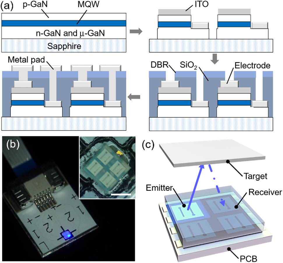
Figure 1.(a) Schematic diagrams showing the fabrication process flow of the GaN chip. (b) Optical image of the packaged chip; inset shows the enlarged image of the chip. Scale bar is 500 μm. (c) Schematic diagram depicting the operating principle of the proximity sensor.
3. Results and Discussion
Figure 1(c) depicts the working mechanism of proximity measurement based on the proposed sensor. The on-chip units based on the InGaN diode structure can operate as an emitter and receiver, connected to a current source and ammeter, respectively. In the InGaN layers of the emitter, light emission is generated through the radiative recombination of the confined carriers. The emitted light can be absorbed by the InGaN layers in the receiver to produce an electron–hole pair due to the partial overlap between the emission and the absorption spectra [26,28,29]. The light propagating through the transparent sapphire substrate experiences varying degrees of reflection, depending on the proximity conditions of the object, and the measured photocurrent can be used to reflect its position changes.
The current-voltage (I-V) properties of the on-chip units are measured by a Keithley 2450 source meter with a resolution of 50 pA. As an emitter, the forward voltage is measured to be 2.80 V at a driving current of 10 mA, as shown in Fig. 2(a). The dynamic resistance extracted from the slope of the linear region of the I-V curve is
![]()
Figure 2.(a)
To investigate the ability of the sensor to detect objects, Al foil, blue- and black-colored films with different reflectance (
![]()
Figure 3.(a) Transient response of the sensor. The emitter is biased with square waves with high voltage levels of 2.8 V, 3.0 V, and 3.2 V. (b) Optical image of the experimental setup used to measure the dynamic response of the sensor. The inset shows a close-up image. (c) Dynamic response measured from an Al foil moving back and forth repeatedly at different distances from the surface of the sensor. Inset shows the schematic of experimental measurement. (d) Measured photocurrent under one cyclic movement of Al foil between
To evaluate the dynamic characteristics of the sensor, a circular Al foil with a diameter of 6 mm is attached to the end of an optical post and a motorized stage (Zolix PSA200-11-X) equipped with a motion controller (Zolix MC600-4B) is used to control the movement of the Al foil, as shown in Fig. 3(b). The instantaneous photocurrent response of the sensor is obtained by moving an Al foil back and forth repeatedly at distances d from the sensors, as illustrated in the inset in Fig. 3(c). For
Having identified that the proposed proximity sensor is highly sensitive to slight distance changes of objects with fast response, the real-time monitoring capability of the chip-scale device in practical applications is studied. Prior to measurement, the target object is affixed with a small piece of Al foil to increase the amount of reflected light. First, the sensor is mounted on a volunteer’s neck and a clear oscillating heart rate signal with a frequency of about 1.3 Hz is obtained, as shown in Figs. 4(a) and 4(d). By enlarging the waveform shown in the inset of Fig. 4(d), detailed information about the blood pressure profile, including a diastolic notch, systolic peak, and diastolic peak can be identified. Then, the sensor is fixed adjacent to the rotary pump, as displayed in Fig. 4(b). It is known that the frequency and amplitude of vibration signal are the key parameters to indicate the operation condition and fault diagnosis of the rotary pump [37], and such noncontact measurement is a direct and simple means. From the results shown in Fig. 4(e), the observation of the sudden increases in photocurrents represents a large extent of vibration at the instant of switching the pump on and off. Between the two distinct on and off signals, a constant frequency of
![]()
Figure 4.Sensor for real-time monitoring. Optical images of the sensor mounted on (a) volunteer’s neck, and close to (b) mechanical pump, (c) speaker diaphragm; (d)–(f) photocurrent profiles measured from the corresponding conditions in (a)–(c); the driving current of the emitter is fixed at 10 mA.
To further testify the ability to detect higher-frequency oscillations, the sensor is mounted close to a commercial speaker with a diameter of 2.9 cm and a working frequency of several hundred hertz, as shown in Fig. 4(c). As illustrated in the plot in Fig. 4(f), the speaker diaphragm vibrating at frequencies of 400, 550, and 700 Hz can be observed. Apart from recognizing the object movement in the vertical direction, detections along the lateral direction are investigated. The sensor is placed close to a white- and black-painted disk equipped on a motorized spinner, as shown in Fig. 5(a). The photocurrent difference of
![]()
Figure 5.(a) Optical image of the sensor mounted close to rotating disk half-painted in black and white; (b) photocurrent profiles measured from the disk at different rotating speeds when the emitter current is 10 mA.
When an on-chip unit acts as an emitter, the others can act as receivers in response to objects in their vicinity. To study this, Al foils of different shapes are placed on the detecting units using the micropositioners (SIGNATONE S-725). As shown in Fig. 6, a sharp contrast of photocurrent levels between the covered and uncovered units can be obtained. For the coverage of a single unit, the photocurrent changes show more than 0.15 μA, which is more than 3 times larger than that of the uncovered ones, as shown in Figs. 6(b)–6(d). Notably, increasing the number of covered units can promote the amount of reflected light, resulting in readout levels exceeding 0.20 and 0.25 μA for double- and triple-covered units, respectively, as shown in Figs. 6(e)–6(g). With the obvious contrast between the measured photocurrents, the sensor can be used to detect small objects overlaid on the units.
![]()
Figure 6.(a) Optical images showing the selective area coverage of the Al foils on the sensor using the micropositioners; distributions of photocurrent changes of units acting as receivers when Al foil is overlaid on (b)–(d) single, (e), (f) double, and (g) triple units. The emitter operates at a low current of 1 mA.
4. Conclusion
In summary, an ultracompact sensor based on the same InGaN/GaN MQW diode structure as the emitters and receiver is demonstrated for proximity measurement. The electrical and optical properties of the on-chip units are investigated, demonstrating the ability to detect objects in the subcentimeter range. The sensor with microsecond response times can respond to the object movements in different dynamic conditions. Fabricated through extendable wafer-scale processes, the proposed proximity sensor provides submillimeter size, fast response, ease of operation, and high repeatability, which makes it well suited for practical applications requiring real-time monitoring.
References
[1] H. K. Lee, S. I. Chang, E. Yoon. Dual-mode capacitive proximity sensor for robot application: implementation of tactile and proximity sensing capability on a single polymer platform using shared electrodes. IEEE Sens. J., 9, 1748-1755(2009).
[2] A. Braun, R. Wichert, A. Kuijper, D. W. Fellner. Capacitive proximity sensing in smart environments. J. Ambient Intell. Smart Environ., 7, 483-510(2015).
[3] Y. Huang, X. Cai, W. Kan, S. Qiu, X. Guo, C. Liu, P. Liu. A flexible dual-mode proximity sensor based on cooperative sensing for robot skin applications. Rev. Sci. Instrum., 88, 085005(2017).
[4] Y. Ye, C. Y. Zhang, C. L. He, X. Wang, J. J. Huang, J. H. Deng. A review on applications of capacitive displacement sensing for capacitive proximity sensor. IEEE Access, 8, 45325-45342(2020).
[5] S. H. Qiu, Y. Huang, X. Y. He, Z. G. Sun, P. Liu, C. X. Liu. A dual-mode proximity sensor with integrated capacitive and temperature sensing units. Meas. Sci. Technol., 26, 105101(2015).
[6] D. J. Sadler, C. H. Ahn. On-chip eddy current sensor for proximity sensing and crack detection. Sens. Actuators A Phys., 91, 340-345(2001).
[7] A. Bonen, R. E. Saad, K. C. Smith, B. Benhabib. A novel electrooptical proximity sensor for robotics: calibration and active sensing. IEEE Trans. Robot., 13, 377-386(1997).
[8] X. Lü, X. Li, F. Zhang, S. Wang, D. Xue, L. Qi, H. Wang, X. Li, W. Bao, R. Chen. A novel proximity sensor based on parallel plate capacitance. IEEE Sens. J., 18, 7015-7022(2017).
[9] J. Castellanos-Ramos, A. Trujillo-León, R. Navas-González, F. Barbero-Recio, J. A. Sánchez-Durán, Ó. Oballe-Peinado, F. Vidal-Verdú. Adding proximity sensing capability to tactile array based on off-the-shelf FSR and PSOC. IEEE Trans. Instrum. Meas., 69, 4238-4250(2019).
[10] L. Sant, A. Fant, S. Stojanovic, S. Fabbro, J. L. Ceballos. A 13.2 b optical proximity sensor system with 130 klx ambient light rejection capable of heart rate and blood oximetry monitoring. IEEE J. Solid-State Circuits, 51, 1674-1683(2016).
[11] C. H. Chen, C. F. Lin, K. H. Wang, H. C. Liu, H. W. Zan, H. F. Meng, W. Hortschitz, H. Steiner, A. Kainz, T. Sauter. High-resolution proximity sensor using flexible semi-transparent organic photo detector. Org. Electron., 49, 305-312(2017).
[12] K. Koyama, M. Shimojo, T. Senoo, M. Ishikawa. High-speed high-precision proximity sensor for detection of tilt, distance, and contact. IEEE Rob. Autom. Lett., 3, 3224-3231(2018).
[13] L. Bürgi, R. Pfeiffer, M. Mücklich, P. Metzler, M. Kiy, C. Winnewisser. Optical proximity and touch sensors based on monolithically integrated polymer photodiodes and polymer LEDs. Org. Electron., 7, 114-120(2006).
[14] M. Prosa, E. Benvenuti, D. Kallweit, P. Pellacani, M. Toerker, M. Bolognesi, L. Lopez-Sanchez, V. Ragona, F. Marabelli, S. Toffanin. Organic light-emitting transistors in a smart-integrated system for plasmonic-based sensing. Adv. Funct. Mater., 31, 2104927(2021).
[15] H. L. Tam, W. H. Choi, F. R. Zhu. Organic optical sensor based on monolithic integration of organic electronic devices. Electronics, 4, 623-632(2015).
[16] A. Laubsch, M. Sabathil, J. Baur, M. Peter, B. Hahn. High-power and high-efficiency InGaN-based light emitters. IEEE Trans. Electron Devices, 57, 79-87(2009).
[17] M. Meneghini, L. R. Trevisanello, G. Meneghesso, E. Zanoni. A review on the reliability of GaN-based LEDs. IEEE Trans. Device Mater. Reliab., 8, 323-331(2008).
[18] M. Meneghini, A. Tazzoli, G. Mura, G. Meneghesso, E. Zanoni. A review on the physical mechanisms that limit the reliability of GaN-based LEDs. IEEE Trans. Electron Devices, 57, 108-118(2009).
[19] D. Chen, D. Li, G. Zeng, F.-C. Hu, Y.-C. Li, Y.-C. Chen, X.-X. Li, J. Tang, C. Shen, N. Chi. GaN-based micro-light-emitting diode driven by a monolithic integrated ultraviolet phototransistor. IEEE Electron Device Lett., 43, 80-83(2021).
[20] S. Hwangbo, L. Hu, A. T. Hoang, J. Y. Choi, J.-H. Ahn. Wafer-scale monolithic integration of full-colour micro-led display using MoS2 transistor. Nat. Nanotechnol., 17, 500-506(2022).
[21] Y. Wang, X. Wang, B. Zhu, Z. Shi, J. Yuan, X. Gao, Y. Liu, X. Sun, D. Li, H. Amano. Full-duplex light communication with a monolithic multicomponent system. Light Sci. Appl., 7, 83(2018).
[22] B. Jia, X. Gao, Z. Ye, P. Liu, F. Hu, H. Zhu, Y. Wang. Monolithically integrated sensing, communication, and energy harvester. Energy Technol., 10, 2100793(2022).
[23] Z. Li, J. Waldron, T. Detchprohm, C. Wetzel, R. Karlicek, T. Chow. Monolithic integration of light-emitting diodes and power metal-oxide-semiconductor channel high-electron-mobility transistors for light-emitting power integrated circuits in GaN on sapphire substrate. Appl. Phys. Lett., 102, 192107(2013).
[24] Y.-J. Lee, Z.-P. Yang, P.-G. Chen, Y.-A. Hsieh, Y.-C. Yao, M.-H. Liao, M.-H. Lee, M.-T. Wang, J.-M. Hwang. Monolithic integration of GaN-based light-emitting diodes and metal-oxide-semiconductor field-effect transistors. Opt. Express, 22, A1589-A1595(2014).
[25] C. Liu, Y. Cai, Z. Liu, J. Ma, K. M. Lau. Metal-interconnection-free integration of InGaN/GaN light emitting diodes with AlGaN/GaN high electron mobility transistors. Appl. Phys. Lett., 106, 181110(2015).
[26] K. H. Li, Y. F. Cheung, W. Jin, W. Y. Fu, A. T. L. Lee, S. C. Tan, S. Y. Hui, H. W. Choi. InGaN RGB light-emitting diodes with monolithically integrated photodetectors for stabilizing color chromaticity. IEEE Trans. Ind. Electron., 67, 5154-5160(2019).
[27] L. Chen, Y. Wu, K. Li. Monolithic InGaN/GaN photonic chips for heart pulse monitoring. Opt. Lett., 45, 4992-4995(2020).
[28] R. Martin, P. Middleton, K. O’Donnell, W. Van der Stricht. Exciton localization and the Stokes’ shift in InGaN epilayers. Appl. Phys. Lett., 74, 263-265(1999).
[29] J. Yan, L. Wang, B. Jia, Z. Ye, H. Zhu, H. Choi, Y. Wang. Uniting GaN electronics and photonics on a single chip. J. Lightwave Technol., 39, 6269-6275(2021).
[30] M. Janecek, W. W. Moses. Optical reflectance measurements for commonly used reflectors. IEEE Trans. Nucl. Sci., 55, 2432-2437(2008).
[31] Y. C. Cai, J. Shen, C. W. Yang, Y. Wan, H. L. Tang, A. A. Aljarb, C. L. Chen, J. H. Fu, X. Wei, K. W. Huang, Y. Han, S. J. Jonas, X. C. Dong, V. Tung. Mixed-dimensional MXene-hydrogel heterostructures for electronic skin sensors with ultrabroad working range. Sci. Adv., 6, eabb5367(2020).
[32] Y. R. Kim, T. L. Phan, K. W. Cho, W. T. Kang, K. Kim, Y. H. Lee, W. J. Yu. Infrared proximity sensors based on photo-induced tunneling in van der Waals integration. Adv. Funct. Mater., 31, 2100966(2021).
[33] V. Kedambaimoole, N. Kumar, V. Shirhatti, S. Nuthalapati, S. Kumar, M. M. Nayak, P. Sen, D. Akinwande, K. Rajanna. Reduced graphene oxide tattoo as wearable proximity sensor. Adv. Electron. Mater., 7, 2001214(2021).
[34] H. Hasegawa, Y. Suzuki, A. G. Ming, K. Koyama, M. Ishikawa, M. Shimojo. Net-structure proximity sensor: high-speed and free-form sensor with analog computing circuit. IEEE/ASME Trans. Mechatron., 20, 3232-3241(2015).
[35] G. S. Lv, H. T. Wang, Y. H. Tong, L. Dong, X. L. Zhao, P. F. Zhao, Q. X. Tang, Y. C. Liu. Flexible, conformable organic semiconductor proximity sensor array for electronic skin. Adv. Mater. Interfaces, 7, 2000306(2020).
[36] K. H. Li, W. Y. Fu, Y. F. Cheung, K. K. Y. Wong, Y. Wang, K. M. Lau, H. W. Choi. Monolithically integrated InGaN/GaN light-emitting diodes, photodetectors, and waveguides on Si substrate. Optica, 5, 564-569(2018).
[37] E. Egusquiza, C. Valero, D. Valentin, A. Presas, C. G. Rodriguez. Condition monitoring of pump-turbines: new challenges. Measurement, 67, 151-163(2015).


Set citation alerts for the article
Please enter your email address

© Copyright 2018-2021 | Chinese Laser Press. All Rights Reserved 沪ICP备15018463号-20