
Xu Wang, Binzhi Zhang. Study on the surface roughness of a high-accuracy optical aspherical mirror fabricated with atmospheric pressure inductively coupled plasma chemical etching technology[J]. Chinese Optics Letters, 2015, 13(Suppl.): S22205
- Chinese Optics Letters
- Vol. 13, Issue Suppl., S22205 (2015)
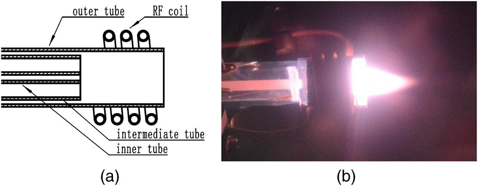
Fig. 1. Three co-axial quartz tube: (a) schematic picture and (b) working picture.
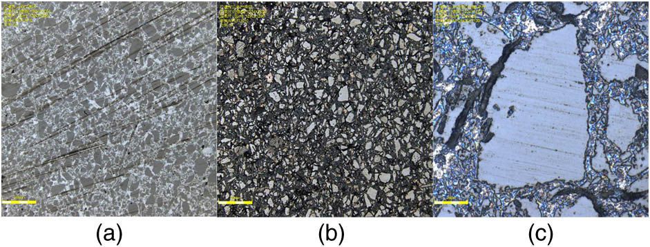
Fig. 2. Microscope testing result on RB–SiC: (a) before PCET (200 × 200 × 2000 ×
Fig. 3. Microscope testing result on S-SiC: (a) before PCET (200 × 2000 × 200 × 2000 ×
Fig. 4. Microscope testing result (200 ×
Fig. 5. Working pictures: (a) Zygo NewView 7200; (b) Mitutoyo Surftest SJ-410.
Fig. 6. Testing result with on fused silica workpiece: (a) Zygo NewView 7200 before fabrication with PCET; (b) Mitutoyo Surftest SJ-410 before fabrication with PCET; (c) Mitutoyo Surftest SJ-410 after fabrication with PCET.
Fig. 7. Testing result with Zygo NewView 7200 on RB-SiC workpiece: (a) before fabrication with PCET; (b) after fabrication with PCET.
Fig. 8. Testing result with Mitutoyo Surftest SJ-410: (a) after fabrication with PCET on RB–SiC workpiece; (b) before PCET on S-SiC sample; (c) after PCET on S-SiC sample.
Fig. 9. Testing result with Zygo NewView 7200 on Si workpiece (unpolished sample after coating on RB–SiC): (a) before fabrication with PCET; (b) after fabrication with PCET.
Fig. 10. Surface roughness of three different materials fabricated with PCET: 1, fused silicon; 2, RB–SiC; 3, S-SiC; 4, Si.
|
Table 1. Experimental Parameters

Set citation alerts for the article
Please enter your email address
© Copyright 2018-2021 | Chinese Laser Press. All Rights Reserved 沪ICP备15018463号-20