
Xu Wang, Binzhi Zhang. Study on the surface roughness of a high-accuracy optical aspherical mirror fabricated with atmospheric pressure inductively coupled plasma chemical etching technology[J]. Chinese Optics Letters, 2015, 13(Suppl.): S22205
- Chinese Optics Letters
- Vol. 13, Issue Suppl., S22205 (2015)
Abstract
Low-pressure plasma technology is very mature in the semiconductor industry and is used in material etching in binary optics. The technology has been divided into capacitively coupled plasma (CCP) and inductively coupled plasma (ICP). The purpose of the technology in binary optics is to create uniform plasma in a bigger space, which could present a better etching effect. The removal rate of the low-pressure plasma is not high enough to fabricate a large aspherical mirror. However, atmospheric pressure plasma has a remarkable removal rate on several optical materials, which is very suitable for fabrication of a large mirror. The disadvantage of atmospheric pressure plasma is that it is too difficult to maintain uniformity in a larger space. To avoid this disadvantage, a three co-axial quarts tubes ICP plasma torch is used to create high temperature and stable plasma in a certain space. Using the given fabrication procedure, it is possible to fabricate a high-accuracy aspherical mirror used in outer space.
Applying atmospheric pressure plasma for fabricating a large optical mirror was developed in the 2000s; its micro-fabricating mechanism is very similar to low-pressure plasma etching.
CCP has been studied by many researchers and has already been applied in many industrial fields, especially in the field of fabricating optical components under vacuum and atmospheric conditions. Wang[
Sign up for Chinese Optics Letters TOC. Get the latest issue of Chinese Optics Letters delivered right to you!Sign up now
ICP is a mature method in spectrum analysis, but it is a brand-new technology in optical fabrication. The RAPT company[
The ICP technology has been developed in Changchun Institute of Optics, Fine Mechanics and Physics (CIOMP) as plasma chemical etching technology (PCET). PCET is used to fabricate kinds of optical materials such as reaction bonded (RB)–SiC, sintered SiC (S-SiC), fused silica, and Si. The removal characteristics of the experiments in CIOMP has been published[
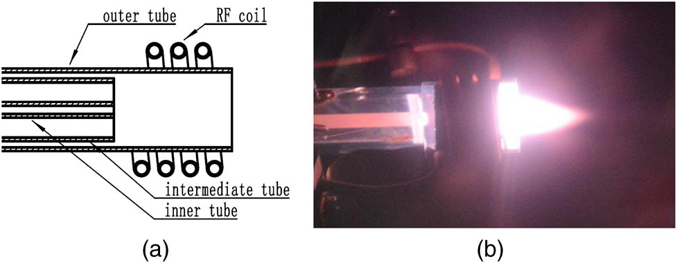
A schematic picture of the front part of the plasma source is given in Fig.
![]()
Figure 1.Three co-axial quartz tube: (a) schematic picture and (b) working picture.
The ICP torch of PCET is driven by the 2000 W RF generator, frequency 27.12 MHz; the plasma source is matched by the matching network of the RF generator. The cooling gas is Ar, the plasma gas is also Ar, and the reactive gas is
| Material | Fused | RB–SiC | Si |
|---|---|---|---|
| RF power (W) | 1000 | 1000 | 1000 |
| Cooling Gas Flow (slm) | 15 | 15 | 15 |
| Plasma Gas Flow (sccm) | 300–2000 | 300–2000 | 300–2000 |
| 0–100 | 0–100 | 0–100 | |
| 0–30 | 0–30 | 0–30 | |
| Working Distance (mm) | 25 | 25 | 25 |
| Sample Temperature (°C) | 215 | 105 | 160 |
Table 1. Experimental Parameters
As far as the experimental results are concerned, the surface roughness will increase after fabrication with PCET. The situation is much more obvious, especially on the RB–SiC wafer. The dual-phase micro-structure (Si phase and SiC phase) of the RB–SiC material is the main cause of the rough surface. The Si phase of the wafer will be removed first, because the Si–Si bond energy is weaker than the Si–C bond energy in the SiC phase. The final fabrication result is that the Si phase is always removed first, which causes micro-indentations on the RB–SiC wafer. Removing the Si phase first will eventually increase the surface roughness, irrespective of the fabrication process. The micro-structure results are observed directly in Fig.
![]()
Figure 2.Microscope testing result on RB–SiC: (a) before PCET (
![]()
Figure 3.Microscope testing result on S-SiC: (a) before PCET (
As for fused silica and silicon, they are all mono-phase materials in theory; the wafer surface roughness fabricated with PCET will be very small. However, in the process of the fabrication, some unknown materials deposit on the wafer, which has a severe influence on the final wafer surface roughness. However, the deposition on the wafer can be removed through a traditional polishing method such as CCOS or MRF. The white material in Fig.
![]()
Figure 4.Microscope testing result (
Based on the experiments and analyses of several materials, and combining CCOS or MRF with PCET, we found that using CCOS or MRF to polish a wafer after PCET is a good method to obtain a smaller surface roughness. This is a new technique combination; the parameters should be optimized to obtain the best fabrication result.
To obtain quantitative results, surface roughness testing experiments were performed on three different wafers fabricated with PCET. Zygo NewView 7200 and Mitutoyo Surface SJ410 were used to test three wafers. The former equipment is used to test a smooth surface; the latter equipment is used to test a rough surface which cannot be tested with an optical method. The working pictures of the testing equipment are displayed in Figs.
![]()
Figure 5.Working pictures: (a) Zygo NewView 7200; (b) Mitutoyo Surftest SJ-410.
![]()
Figure 6.Testing result with on fused silica workpiece: (a) Zygo NewView 7200 before fabrication with PCET; (b) Mitutoyo Surftest SJ-410 before fabrication with PCET; (c) Mitutoyo Surftest SJ-410 after fabrication with PCET.
![]()
Figure 7.Testing result with Zygo NewView 7200 on RB-SiC workpiece: (a) before fabrication with PCET; (b) after fabrication with PCET.
![]()
Figure 8.Testing result with Mitutoyo Surftest SJ-410: (a) after fabrication with PCET on RB–SiC workpiece; (b) before PCET on S-SiC sample; (c) after PCET on S-SiC sample.
![]()
Figure 9.Testing result with Zygo NewView 7200 on Si workpiece (unpolished sample after coating on RB–SiC): (a) before fabrication with PCET; (b) after fabrication with PCET.
As far as the fused silica wafer is concerned, there is too much deposition on the wafer fabricated with PCET to be tested by Zygo NewView 7200; consequently, Mitutoyo Surface SJ410 is a better option; the testing result is displayed in Fig.
Figure
![]()
Figure 10.Surface roughness of three different materials fabricated with PCET: 1, fused silicon; 2, RB–SiC; 3, S-SiC; 4, Si.
Analyzing the testing results, the wafer surface roughness increases after fabrication with PCET. The fused silica wafer roughness increases 5 times. If the fused silica wafer is fabricated with PCET first, then polished with CCOS or MRF after the PCET procedure, this will result in a better surface quality (i.e., reduced surface roughness). In the process of CCOS or MRF, the deposition on the wafer will be removed quickly. The RB–SiC wafer surface roughness increases rapidly, almost 40 times. On the contrary, the S-SiC wafer roughness does not change obviously, only 1.07 times. Compared with an RB–SiC wafer, the situation of the Si wafer is much better; the surface roughness only increased to twice that which it had been previously. The surface roughness measurement results of four wafers prove the validity of the aforementioned hypothesis. The dual-phase material surface roughness increases rapidly after fabrication with PCET. However, the main reason why the mono-phase material surface roughness increases is that the reaction products deposit on the wafer.
The Letter is focused on a new inductively coupled PCET operating at atmospheric pressure. PCET is a successful method in terms of fabricating fused silica, RB–SiC, S-SiC, and a Si optical mirror. It has much potential compared with CCOS and IBF. The surface roughness experiments are carried out on four different material wafers. After PCET experiments, it is found that the wafer surface roughness all increased to different extents. As far as mono-phase materials such as fused silica and Si are concerned, the main reason for the roughness increase is the fluoride deposition on the wafer surface during the fabrication process. The fluoride deposition can be completely removed by use of CCOS or MRF. The S-SiC is a mono-phase material; the micro-hole structure emerges on the S-SiC wafer surface after fabrication with PCET, which slightly increases the wafer surface roughness. As for RB–SiC, it is a dual-phase material; typically, the Si-phase material removal rate is higher than the SiC-phase in the plasma circumstance, which leads to the emergence of indentations on the wafer surface. Consequently, the RB–SiC wafer surface roughness clearly increases after fabrication with PCET. Overall, the reason for the wafer surface roughness increase is deduced through examining the wafer micro-structure. Combining the advantages of the PCET high removal rate and CCOS or MRF readily yielding an excellent mirror surface roughness, the PCET has great promise in terms of fabricating a large aspherical mirror.
References
[1] Y. Wang, L. Hang, M. Hu. Surf. Technol., 37, 51(2008).
[2] J. Wang, B. Wang, J. Zhang, S. Dong. Aviation Precis. Manuf. Technol., 44, 11(2008).
[4] H. Takino, K. Yamamura, Y. Sano, Y. Mori. Appl. Opt., 49, 4434(2010).
[6] I. Eichentopf, G. Böhm, T. Arnold. Surf. Coat. Technol., 205, S430(2011).
[7] I. Eichentopf, G. Böhm, J. Meister, T. Arnod. Plasma Process. Polym., 6, S204(2009).
[9] P. K. Subrahmanyan, G. Gardopee. Proc. SPIE, 7018, 701809(2008).
[11] M. Castelli, R. Jourdain, P. Morantz, P. Shore. Prec. Eng., 36, 467(2012).
[13] W. O’Brien. Characterisation and material removal properties of the RAP™ process(2011).

Set citation alerts for the article
Please enter your email address
© Copyright 2018-2021 | Chinese Laser Press. All Rights Reserved 沪ICP备15018463号-20