• Photonics Research
  • Vol. 4, Issue 6, 272 (2016)
Tae-Woo Lee, Da Eun Lee, Young Jin Lee, and Soon-Hong Kwon*
Author Affiliations
  • Department of Physics, Chung-Ang University, Seoul 06974, South Korea
  • show less
    DOI: 10.1364/PRJ.4.000272 Cite this Article Set citation alerts
    Tae-Woo Lee, Da Eun Lee, Young Jin Lee, Soon-Hong Kwon. Low cross-talk, deep subwavelength plasmonic metal/insulator/metal waveguide intersections with broadband tunability[J]. Photonics Research, 2016, 4(6): 272 Copy Citation Text show less
    (a) Schematic diagram of two conventional plasmonic MIM crossed waveguides. (b) Side-view and top-view of the mode profile (Ez) in the x−y plane at the center of an air gap with a gap thickness of 10 nm.
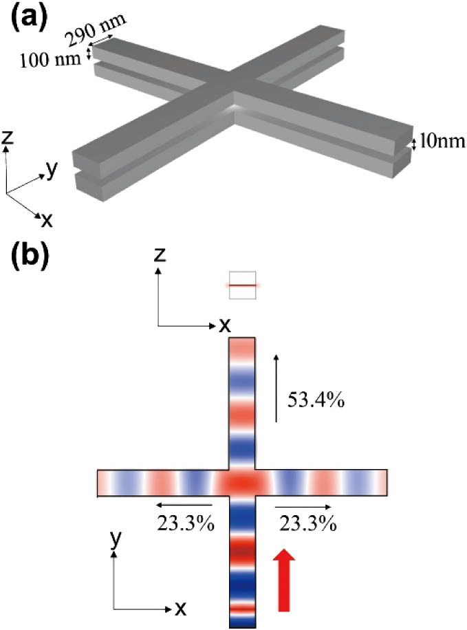
    Fig. 1. (a) Schematic diagram of two conventional plasmonic MIM crossed waveguides. (b) Side-view and top-view of the mode profile (Ez) in the xy plane at the center of an air gap with a gap thickness of 10 nm.
    (a) Schematic diagram of a double silver block cavity. Each block has dimensions of 250 nm×250 nm×100 nm. The mode profiles of the vertical electric field component (Ez) of the plasmonic cavity mode: (b) top-view of the x−y plane at the center of the air gap, (c) side-view of the y−z plane, and (d) x′−z plane at the center of the blocks. (e) Resonances of the cavity mode for different gap thicknesses from 6 nm (black) to 14 nm (green). (f) Resonant wavelength of the cavity mode as a function of the gap thickness.
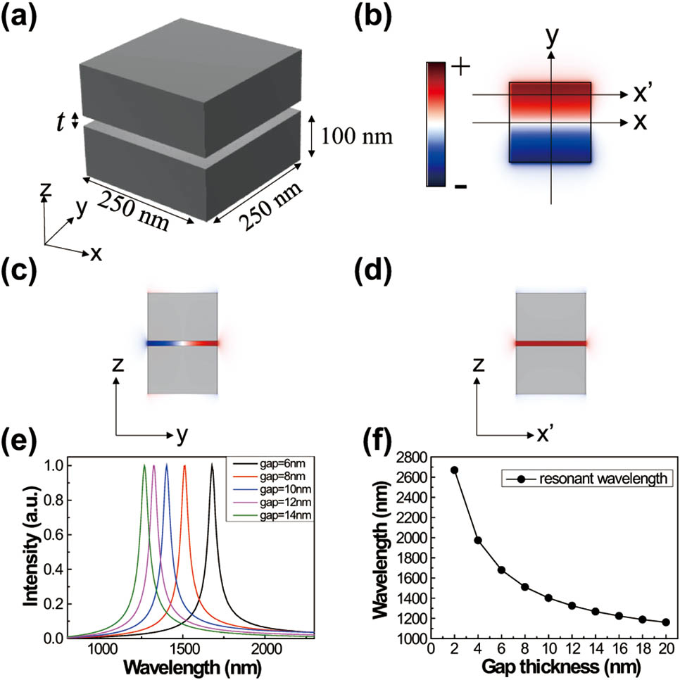
    Fig. 2. (a) Schematic diagram of a double silver block cavity. Each block has dimensions of 250  nm×250  nm×100  nm. The mode profiles of the vertical electric field component (Ez) of the plasmonic cavity mode: (b) top-view of the xy plane at the center of the air gap, (c) side-view of the yz plane, and (d) xz plane at the center of the blocks. (e) Resonances of the cavity mode for different gap thicknesses from 6 nm (black) to 14 nm (green). (f) Resonant wavelength of the cavity mode as a function of the gap thickness.
    (a) MIM waveguide consisting of two silver strips with an air gap thickness of t. The gray plane represents the x−y plane at the center of the air gap. The mode profiles of the (b) even and (c) odd waveguide modes at the gray plane. Dispersion relations of (d) even and (e) odd modes of waveguides where w=200 nm (black) and w=330 nm (red). Horizontal black dashed line represents a target wavelength of 1550 nm (2πf=1215 THz).
    Fig. 3. (a) MIM waveguide consisting of two silver strips with an air gap thickness of t. The gray plane represents the xy plane at the center of the air gap. The mode profiles of the (b) even and (c) odd waveguide modes at the gray plane. Dispersion relations of (d) even and (e) odd modes of waveguides where w=200  nm (black) and w=330  nm (red). Horizontal black dashed line represents a target wavelength of 1550 nm (2πf=1215  THz).
    (a) Schematic of the proposed tunable low cross-talk cross-connector consisting of a square cavity and four-port waveguides. The Ez mode profiles of the cavity mode in the cross-connector for different geometrical factors: (b) one side (Wc) of the square cavity is 300 nm and the waveguide width (Wwg) is 330 nm and (c) Wc and Wwg are 250 and 200 nm, respectively. The air gap (t) of the cavity and the air gap of the waveguide are 10 nm. The cavity is separated from the waveguides by 15 nm. Dotted lines 500 nm away from the air spaces between cavity and waveguides indicate the position where power flows are calculated.
    Fig. 4. (a) Schematic of the proposed tunable low cross-talk cross-connector consisting of a square cavity and four-port waveguides. The Ez mode profiles of the cavity mode in the cross-connector for different geometrical factors: (b) one side (Wc) of the square cavity is 300 nm and the waveguide width (Wwg) is 330 nm and (c) Wc and Wwg are 250 and 200 nm, respectively. The air gap (t) of the cavity and the air gap of the waveguide are 10 nm. The cavity is separated from the waveguides by 15 nm. Dotted lines 500 nm away from the air spaces between cavity and waveguides indicate the position where power flows are calculated.
    (a) SPP waveguide modes pass through the cross-connector without cross-talk. The side of the cavity and the waveguide width are 250 and 200 nm, respectively, similar to Fig. 4(c). (b) Resonant wavelengths of the isolated cavity (black) and the cavity with four-port waveguides (red) as a function of the air gap thickness (t). (c) Transmission spectra and cross-talk spectra in the cross-connector for different air gap thicknesses from 4 nm (violet) to 14 nm (green). The cross-talk curves are plotted inside the black circle. (d) Resonant wavelength shifts (black) and transmission ratios (blue) in the cross-connector as a function of the air gap thickness. The wavelength shift (Δλ) is defined as the change in the resonance from the resonant wavelength of the cavity with an air gap thickness of 10 nm.
    Fig. 5. (a) SPP waveguide modes pass through the cross-connector without cross-talk. The side of the cavity and the waveguide width are 250 and 200 nm, respectively, similar to Fig. 4(c). (b) Resonant wavelengths of the isolated cavity (black) and the cavity with four-port waveguides (red) as a function of the air gap thickness (t). (c) Transmission spectra and cross-talk spectra in the cross-connector for different air gap thicknesses from 4 nm (violet) to 14 nm (green). The cross-talk curves are plotted inside the black circle. (d) Resonant wavelength shifts (black) and transmission ratios (blue) in the cross-connector as a function of the air gap thickness. The wavelength shift (Δλ) is defined as the change in the resonance from the resonant wavelength of the cavity with an air gap thickness of 10 nm.
    Tae-Woo Lee, Da Eun Lee, Young Jin Lee, Soon-Hong Kwon. Low cross-talk, deep subwavelength plasmonic metal/insulator/metal waveguide intersections with broadband tunability[J]. Photonics Research, 2016, 4(6): 272
    Download Citation