Abstract
We suggest a low cross-talk plasmonic cross-connector based on a metal/insulator/metal cavity and waveguides. We separately investigate the isolated cavity mode, the waveguide mode, and the combination of cavity and waveguide modes using a finite-different time-domain method. Due to resonant tunneling and the cutoff frequency of the odd waveguide mode, our proposed structure achieves a high throughput transmission ratio and eliminates cross-talk. Furthermore, the proposed structure has a broadband tunability of 587 nm, which can be achieved by modulating the cavity air gap thickness. This structure enables the miniaturization of photonic integrated circuits and sensing applications.1. INTRODUCTION
Surface plasmon polaritons (SPPs) are propagating collective oscillations that are electromagnetic waves coupled with free electrons between a dielectric and a metallic interface. Compared to conventional optics, SPPs can manipulate light beyond the subwavelength regime. This is because the field confinement of SPPs overcomes the diffraction limit of light near the surface plasmon frequency [1–15]. Recent studies have demonstrated the application of plasmonic devices such as optical switches [2,3], biochemical sensors [4,5], and advanced displays [6,7]. Plasmonic waveguides [5,8–13] are another example of plasmonic applications. Due to their subwavelength mode confinement, SPP waveguides are among the best candidates for compact photonic integrated circuits (PICs). In SPP waveguides, the trade-off between the lateral confinement and propagation length is determined by the geometry. Metal/insulator/metal (MIM) waveguides are suitable for optical data transmission in PICs because of their deep subwavelength modal area, strong confinement, and relatively long propagation length [10–14]. In order to construct more compact and less complex PICs, it is also necessary to intersect waveguide devices [13,16–18]. In addition, for efficient signal transduction, SPPs must be able to propagate in a desired direction. Therefore, elimination of cross-talk must be achieved.
In photonic crystal waveguides, low cross-talk structures have been proposed based on the resonant tunneling and mode symmetry [16,17]. Minimizing cross-talk in the metal slot waveguides and dielectric ridge waveguides has also been studied [13,18]. However, previous research was mostly limited in two-dimensional (2D) simulations, which cannot consider radiation loss. Also, the previous crossing regions to minimize cross-talk usually had a size of several micrometers or at least a wavelength. Only a few three-dimensional (3D) studies on low cross-talk cross-connecting waveguides with deep subwavelength size have been reported [19].
In order to understand the transmission properties of conventional cross-connected MIM waveguides, we investigated the transmission properties of a system consisting of two MIM waveguides that are orthogonally crossed, as shown in Fig. 1(a). Each MIM waveguide consists of two silver strips with a width of 290 nm and a thickness of 100 nm; these are separated by an air gap with a size of 10 nm. In this MIM structure, the SPP waveguide mode with a target wavelength of 1550 nm () is tightly confined inside of the air gap [side-view of Fig. 1(b)]. The cross-sectional physical mode area is , which is a deep subwavelength size of . In this structure, when the SPP mode is injected from one of the waveguides, as shown in the top-view of Fig. 1(b), 53.4% of the mode energy transmits through the junction to the straight arm waveguide and 46.6% of the mode propagates to the two orthogonal waveguides. This large cross-talk (46.6%) will lower the signal to the desired waveguide (i.e., the straight waveguide) and cause a large amount of noise in unwanted waveguides (i.e., the orthogonal waveguides). The cross-talk can be suppressed by introducing a cavity and using resonant tunneling and mode symmetry [16,17]. In addition, the cutoff frequency of the waveguide mode will prevent coupling with unwanted waveguides.
Sign up for Photonics Research TOC. Get the latest issue of Photonics Research delivered right to you!Sign up now
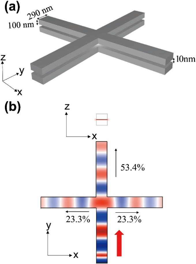
Figure 1.(a) Schematic diagram of two conventional plasmonic MIM crossed waveguides. (b) Side-view and top-view of the mode profile () in the plane at the center of an air gap with a gap thickness of 10 nm.
In this article, we propose a theoretical tunable cross-connector, which transmits a signal into the desired waveguide with low cross-talk using resonant tunneling and the symmetries of the cavity and waveguide modes. The transmitting wavelength can be tuned over a broad spectral range (500 nm) with a center wavelength of 1550 nm. This is done by adjusting the air gap of the cavity placed at the waveguide intersection. Broadband light is injected, and the transmitting signal and cross-talk are investigated based on a 3D finite-difference time-domain (FDTD) method. The silver is represented by the Drude model, which is described as follows:
The background dielectric constant (), plasma frequency (), and collision frequency () are determined by the dielectric constant of silver; these values are set to 3.140, 0.021 eV, and 9.130 eV, respectively [5,12,14,15,20].
2. MAIN
In order to eliminate cross-talk, a resonant cavity can be used as a junction for resonant tunneling. We use a rectangular cavity structure [14] that consists of two silver blocks that are each . The two nano-blocks are separated by a deep subwavelength air gap with a thickness of . Figure 2(a) shows the schematic diagram of the proposed cavity structure without waveguides. In this cavity, a plasmonic MIM mode with an -dominant field is excited at 1402 nm, as shown in the mode profile of Fig. 2(b). The mode has one intensity node along the axis and a degenerate mode with a node along the axis. The cavity mode is strongly confined inside the air gap. As shown Fig. 2(b), the cavity has different mode symmetry about the and axes. For the axis, the cavity has odd mirror symmetry, whereas the cavity has even mirror symmetry for the axis. Figures 2(c) and 2(d) represent the side-views of each mode, respectively.

Figure 2.(a) Schematic diagram of a double silver block cavity. Each block has dimensions of . The mode profiles of the vertical electric field component () of the plasmonic cavity mode: (b) top-view of the plane at the center of the air gap, (c) side-view of the plane, and (d) plane at the center of the blocks. (e) Resonances of the cavity mode for different gap thicknesses from 6 nm (black) to 14 nm (green). (f) Resonant wavelength of the cavity mode as a function of the gap thickness.
To investigate spectral properties of the proposed cavity, we calculate the resonant spectrum of the cavity for different gap sizes from 6 to 14 nm. Figure 2(e) shows the resonant spectrum of the cavity for different gap thicknesses. The resonant wavelength is strongly dependent on the gap size. As the gap size decreases, the resonant peak shifts to a longer wavelength. This is because the effective refractive index of the cavity increases as the gap thickness decreases [14]. In order to find the resonant wavelength shift for different gap thicknesses, we investigate the resonant peak by changing the gap thickness between 2 and 20 nm, as shown in Fig. 2(f). As the gap thickness decreases, the resonant wavelength increases drastically; this is caused by stronger plasmonic coupling. For a cavity with , the cavity mode has a resonant wavelength of 1161 nm, and for a cavity with , the cavity mode has a resonant wavelength of 2669 nm. Upon an 18 nm change in the air gap thickness, a large wavelength shift of 1508 nm is observed. This result shows that the resonant wavelength can be tuned over a broad range by controlling the cavity air gap thickness.
In plasmonic systems, loss can be divided into radiation loss and metallic absorption loss. In the proposed MIM waveguide, radiation loss is negligible due to the high effective index of the waveguide mode. On the other hand, in the cavity in Fig. 2, radiation loss is 20% of the total loss.
To design a low cross-talk cross-connector, the optical properties of odd and even waveguides are also investigated for different waveguide widths. The MIM waveguide consists of two silver strips with a width of and a height of . The strips are separated by an air gap with a thickness of . In this article, the height and the thickness of the air gap of the waveguide are set to 100 and 10 nm, respectively. There exist two waveguide modes depending on the symmetry in this MIM waveguide. Figures 3(b) and 3(c) show the mode profile of even and odd waveguide modes, which have even and odd mirror symmetries about the propagation direction, respectively. In these figures, each waveguide mode profile is obtained at a wavelength of 1550 nm for a waveguide that is 330 nm wide. The two types of waveguide modes have different dispersion relations [12]. In Fig. 3(d), dispersion curves of the even waveguide mode changed slightly as the width of the waveguide changed from 330 to 220 nm. In the even waveguide mode, propagation of SPPs is allowed for the entire frequency range. Contrary to the even waveguide mode, the odd waveguide mode has a strong width-dependence. As shown in Fig. 3(e), the dispersion curves of the odd waveguide mode have cutoff frequencies that changed largely as the width of the waveguide changed. The SPP waveguide mode, which has a lower frequency than the cutoff frequency, cannot propagate. Because the dispersion of the odd waveguide mode moves upward for smaller waveguide widths, the allowed frequency region for odd mode propagation can be reduced with smaller waveguide widths. In this simulation, cutoff frequencies (cutoff wavelengths) are calculated as 1744 THz (1080 nm) and 1123 THz (1675 nm) for waveguide widths of 200 and 330 nm, respectively. For (), the even waveguide mode can propagate in both of the waveguides. However, due to the cutoff frequency of the odd waveguide mode, SPP with 1550 nm propagates only in the 330-nm-wide waveguide.
Figure 3.(a) MIM waveguide consisting of two silver strips with an air gap thickness of t. The gray plane represents the plane at the center of the air gap. The mode profiles of the (b) even and (c) odd waveguide modes at the gray plane. Dispersion relations of (d) even and (e) odd modes of waveguides where (black) and (red). Horizontal black dashed line represents a target wavelength of 1550 nm ().
In the conventional plasmonic MIM cross-connector, high cross-talk is observed in Fig. 1. In order to solve this problem, a resonant cavity is placed at the center of the intersection. When the cavity is located at the center of the intersection, and one cavity mode is excited, the coupling between four-port waveguides and the cavity mode is investigated for different cavity and waveguide sizes. As shown in Fig. 2(b), the cavity mode has even mirror symmetry about the axis and odd mirror symmetry about the axis. In Fig. 4(a), the cavity has a square cross-section (sized by ), a height of 100 nm, and an air gap of 10 nm. The gap between the cavity and the waveguides is set to 15 nm.
In order to understand couplings between the cavity and different waveguide widths, the cavity mode is excited by placing an dipole source at the antinode of the cavity mode, and the coupled energy to each waveguide is calculated. Figure 4(b) represents the profile of the wide waveguides () and the cavity (, ). When the cavity mode with a wavelength of 1662 nm is excited, the even waveguide modes are excited in the up and down waveguides and the odd waveguide modes are excited in the left and right waveguides. The coupling ratios between the cavity and the wide waveguide along the and axes are calculated to be 74.8% and 25.2%, respectively. As the next step to eliminate cross-talk, we modulate the cavity width and waveguide width to use the cutoff frequency of the odd mode. Figure 4(c) shows the profile of the narrow waveguides () and the cavity (, ). In the same manner as shown in Fig. 4(b), we calculate the coupling ratios between the cavity and the waveguides. In this structure, a cavity mode is excited with a wavelength of 1562 nm. The couplings to the odd waveguide modes of the left and right waveguides are forbidden since the cutoff wavelength of the odd waveguide mode is 1080 nm in the 250-nm-wide waveguide. In contrast, the couplings to the up and down waveguides are allowed due to the absence of a cutoff in the even waveguide; almost 50% of the energy is delivered into each waveguide. Only 0.00025% of the energy is transferred into the left and right waveguides. It is expected that the proposed structure can be used as a high transmission and low cross-talk cross-connector.
Figure 4.(a) Schematic of the proposed tunable low cross-talk cross-connector consisting of a square cavity and four-port waveguides. The mode profiles of the cavity mode in the cross-connector for different geometrical factors: (b) one side () of the square cavity is 300 nm and the waveguide width () is 330 nm and (c) and are 250 and 200 nm, respectively. The air gap () of the cavity and the air gap of the waveguide are 10 nm. The cavity is separated from the waveguides by 15 nm. Dotted lines 500 nm away from the air spaces between cavity and waveguides indicate the position where power flows are calculated.
Based on the structure in Fig. 4(c), we investigated the transmission properties from one input waveguide to one of the other waveguides. In the certain positions, 500 nm away from the air spaces between cavity and waveguides, Poynting vectors passing through the planes with a size of orthogonal to the direction of the waveguide arm were calculated to estimate power flows to each waveguide arm. When an even SPP waveguide mode with a wavelength of 1562 nm (i.e., the resonant wavelength of the cavity) is injected from the bottom waveguide, a high transmission ratio (75.6%) and a small amount of cross-talk (1%) to the left and right waveguides are estimated, as shown in the mode profile of Fig. 5(a). This is because the even waveguide mode excites the cavity mode with even (odd) mirror symmetry along the axis via resonant tunneling. Therefore, the cavity mode can couple to only the up waveguide due to the cutoff frequency of the odd waveguide mode in the left/right waveguides. Alternatively, the strong wavelength dependence on the air gap of the cavity enables the proposed structure to be used as a tunable optical filter. Figure 5(b) shows the resonant wavelengths of the isolated cavity as shown in Fig. 2(a) and the proposed structure shown in Fig. 4(c) as a function of the cavity air gap thickness with a fixed waveguide gap. Here, the air gaps of four waveguides are fixed to 10 nm. Because the four waveguide ports surrounding the cavity affect the resonant wavelength of the proposed structure, the resonant wavelengths of the proposed structure are slightly shifted to longer wavelengths. When the cavity gap thickness decreases from 20 to 2 nm, the resonant wavelength of the proposed structure is calculated to shift from 1414 to 2713 nm. Because SPPs can be transmitted between the waveguide and the cavity via resonant tunneling, we believe that the proposed structure can be operated in the desired wavelength regime by modulating the cavity gap thickness. Figure 5(c) shows the transmission and cross-talk spectra of the proposed structure for different cavity air gap thicknesses ranging from 4 to 14 nm. The transmission spectrum is a single peak, and the peak shifts to shorter wavelength as the gap increases. Indeed, each transmission peak completely matches with the resonant wavelength of the proposed structure. Compared to the throughput transmittance, the cross-talk can be ignored ( for the whole wavelength region). Figure 5(d) shows the resonant shifts and throughput transmission ratios for different cavity air gap thicknesses from 4 to 14 nm. The resonant wavelength shift () is defined as [resonant wavelength of a cavity air gap thickness of ]—[resonant wavelength of a cavity air gap thickness of 10 nm ], where is 1562 nm. At a cavity gap thickness of 14 nm, the transmission peak wavelength is 1468 nm () and the transmission ratio is 78%. For a gap thickness of 4 nm, the peak wavelength is 2055 nm () and the transmission ratio is 57%. By modulating the cavity air gap thickness from 4 to 14 nm, a broad tuning range of 587 nm with a transmission ratio larger than 57% can be achieved. The transmission ratio tends to decrease as the cavity air gap thickness decreases. This is because the metallic absorption loss of the cavity nonlinearly increases as the cavity thickness decreases [14], which can be reduced by using hybrid SPP waveguides [15].
Figure 5.(a) SPP waveguide modes pass through the cross-connector without cross-talk. The side of the cavity and the waveguide width are 250 and 200 nm, respectively, similar to Fig. 4(c). (b) Resonant wavelengths of the isolated cavity (black) and the cavity with four-port waveguides (red) as a function of the air gap thickness (). (c) Transmission spectra and cross-talk spectra in the cross-connector for different air gap thicknesses from 4 nm (violet) to 14 nm (green). The cross-talk curves are plotted inside the black circle. (d) Resonant wavelength shifts (black) and transmission ratios (blue) in the cross-connector as a function of the air gap thickness. The wavelength shift () is defined as the change in the resonance from the resonant wavelength of the cavity with an air gap thickness of 10 nm.
3. CONCLUSION
In this article, we proposed a low cross-talk tunable plasmonic MIM cross-connector that consists of a double silver block cavity and four MIM waveguide ports. The SPP propagation mode properties are determined by the cavity and waveguide mode symmetries and by the cutoff frequency of the waveguide mode. Therefore, SPPs propagate into the throughput waveguide with an even waveguide mode and propagate into the transverse waveguide with an odd waveguide mode. The cross-talk, where light propagates to the transverse waveguides, is eliminated by the cutoff frequency of the odd waveguide mode. Compared with the throughput transmittance and cross-talk of conventional MIM waveguides, the proposed structure has a higher throughput transmission ratio and less cross-talk. Furthermore, the proposed structure has large tunability from 1468 to 2055 nm, which is obtained by modulating the cavity air gap thickness from 14 to 4 nm. The proposed structure provides high transmission to the desired waveguide and low cross-talk to unwanted waveguides at the intersection of two waveguides. This can be exploited to build high density PICs. In addition, the large tunability of the operating wavelength channel and the extreme sensitivity (587 nm/10 nm) to the air gap thickness of the cavity suggest that the proposed structure can be used as a tunable optical filter as well as an angstrom-resolution air gap sensor.
In order to consider the practicality of a real device based on the suggested architecture, one can take into account substrate, different gap material, and surrounding materials. Practically, a substrate-supported structure can be considered while the optical performance of the free-standing structure is maintained because of strong field concentration between silver blocks. For the mechanically solid structure, dielectric material can be assumed for the gap material instead of air. Therefore, we investigated the optical performance in the case of gap material. Because of the higher index, the structure in the gap system decreases with the cavity size () of 200 nm and waveguide width () of 180 nm from and in the air gap system. Here, the gap size and air spacing are fixed to 10 and 15 nm. In the gap system, low cross-talk operation is maintained by the mechanism of cutoff frequency and mode symmetry while slightly larger coupling energy of 0.10% is transferred into the left and right waveguides in the same geometry of Fig. 4(c). On the other hand, when nonlinear material is applied as the gap material, the proposed structure can be used for a low operating power optical switch [21]. If higher index surrounding material such as water instead of air is assumed, more radiation loss is caused due to weaker plasmonic confinement while low cross-talk operation is maintained.
References
[1] D. K. Gramotnev, S. I. Bozhevolnyi. Plasmonics beyond the diffraction limit. Nat. Photonics, 4, 83-91(2010).
[2] G. Wang, H. Lu, X. Liu, Y. Gong. Numerical investigation of an all-optical switch in a graded nonlinear plasmonic grating. Nanotechnology, 23, 4440009(2012).
[3] N. Jiang, L. Shao, J. Wang. (Gold nanorod core)/(Polyaniline shell) plasmonic switches with large plasmon shifts and modulation depths. Adv. Mater., 26, 3282-3289(2014).
[4] N. Liu, M. L. Tang, M. Hentschel, H. Giessen, A. P. Alivisatos. Nanoantenna-enhanced gas sensing in a single tailored nanofocus. Nat. Mater., 10, 631-636(2011).
[5] D. E. Lee, T.-W. Lee, S.-H. Kwon. Spatial mapping of refractive index based on a plasmonic tapered channel waveguide. Opt. Express, 23, 5907-5914(2015).
[6] K. Okamoto, I. Niki, A. Shvartser, Y. Narukawa, T. Mukai, A. Scherer. Surface-plasmon-enhanced light emitters based on InGaN quantum wells. Nat. Mater., 3, 601-605(2004).
[7] L.-W. Jang, D.-W. Jeon, M. Kim, J.-W. Jeon, A. Y. Polyakov, J.-W. Ju, S.-J. Lee, J.-H. Baek, J.-K. Yang, I.-H. Lee. Investigation of optical and structural stability of localized surface plasmon meditated light-emitting diodes by Ag and Ag/SiO2 nanoparticles. Adv. Funct. Mater., 22, 2728-2734(2012).
[8] V. A. Zenin, V. S. Volkov, Z. Han, S. I. Bozhevolnyi, E. Devaux, T. W. Ebbesen. Dispersion of strongly confined channel plasmon polariton modes. J. Opt. Soc. Am. B, 28, 1596-1602(2011).
[9] R. F. Oulton, V. J. Sorger, D. A. Genov, D. F. P. Pile, X. Zhang. A hybrid plasmonic waveguide for subwavelength confinement and long-range propagation. Nat. Photonics, 2, 496-500(2008).
[10] J. A. Dionne, L. A. Sweatlock, H. A. Atwater. Plasmon slot waveguides: towards chip-scale propagation with subwavelength-scale localization. Phys. Rev. B, 73, 035407(2006).
[11] Y. Liu, F. Zhou, B. Yao, J. Cao, Q. Mao. High-extinction-ratio and low insertion-loss plasmonic filter with coherent coupled nano-cavity array in a MIM waveguide. Plasmonics, 8, 1035-1041(2013).
[12] T.-W. Lee, D. E. Lee, S.-H. Kwon. Dual-function metal-insulator-metal plasmonic optical filter. IEEE Photon. J., 7, 4800108(2015).
[13] S. Xiao, N. A. Mortensen. Resonant-tunneling-assisted crossing for subwavelength plasmonic slot waveguides. Opt. Express, 16, 14997-15005(2008).
[14] S.-H. Kwon. Plasmonic ruler with angstrom distance resolution based on double metal blocks. IEEE Photon. Technol. Lett., 25, 1619-1622(2013).
[15] J.-H. Kang, H.-G. Park, S.-H. Kwon. Room-temperature high-Q channel-waveguide surface plasmon nanocavity. Opt. Express, 19, 11892-13898(2011).
[16] S. G. Johnson, C. Manolatou, S. Fan, P. R. Villeneuve, J. D. Joannopoulos. Elimination of cross talk in waveguide intersections. Opt. Lett., 23, 1855-1857(1998).
[17] S.-H. Kwon, M. Kamp, A. Forchel, M.-K. Seo, Y.-H. Lee. Elimination of cross-talk in waveguide intersections of triangular lattice photonic crystals. Opt. Express, 16, 11399-11404(2008).
[18] W. Bogaerts, P. Dumon, D. V. Thourhout, R. Baets. Low-loss, low-cross-talk crossings for silicon-on-insulator nanophotonic waveguides. Opt. Lett., 32, 2801-2803(2007).
[19] A. Mahigir, P. Dastmalchi, W. Shin, S. Fan, G. Veronis. Plasmonic coaxial waveguide-cavity devices. Opt. Express, 23, 20549-20562(2015).
[20] P. B. Johnson, R. W. Christy. Optical constants of the noble metals. Phys. Rev. B, 6, 4370-4379(1972).
[21] Y. Shen, G. P. Wang. Optical bistability in metal gap waveguide nanocavities. Opt. Express, 16, 8421-8426(2008).


