
Lucas Deniel, Erwan Weckenmann, Diego Pérez Galacho, Christian Lafforgue, Stéphane Monfray, Carlos Alonso-Ramos, Laurent Bramerie, Frédéric Boeuf, Laurent Viven, Delphine Marris-Morini. Silicon photonics phase and intensity modulators for flat frequency comb generation[J]. Photonics Research, 2021, 9(10): 2068
- Photonics Research
- Vol. 9, Issue 10, 2068 (2021)
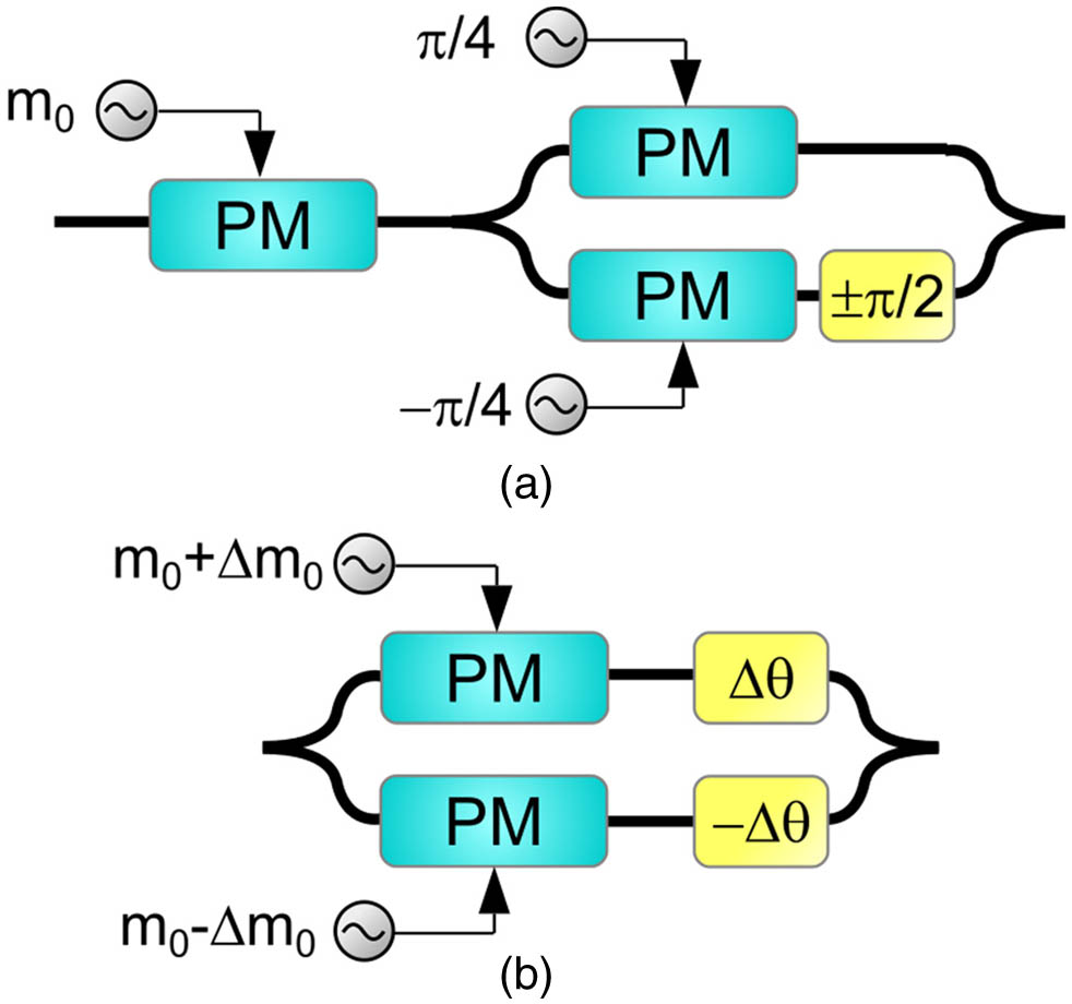
Fig. 1. Schematic of (a) the PM-MZM and (b) the DD-MZM structures. Under specific phase modulation indices and static optical phase shifts, these structures produce tunable flat EO-FCs. (PM, phase modulator.)
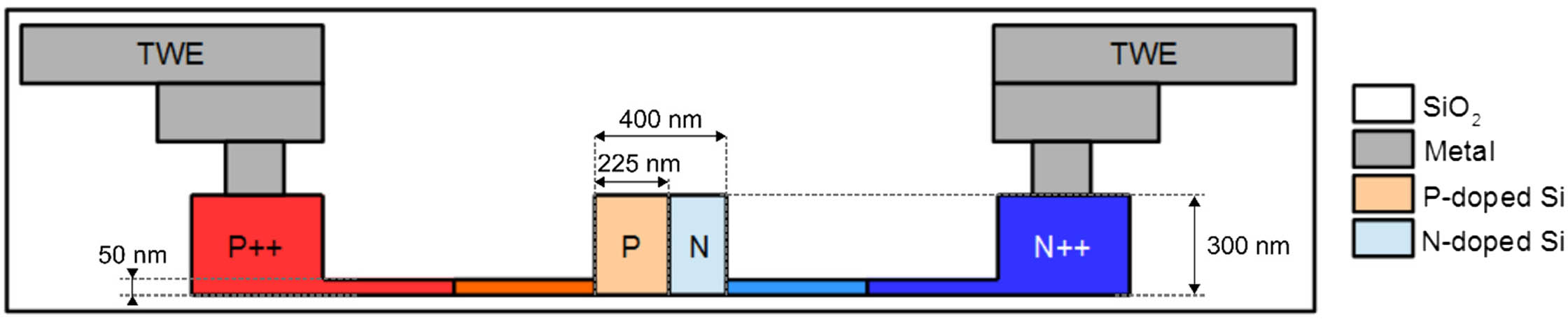
Fig. 2. Schematic cross section of the phase modulator. A PN junction is created in the waveguide to leverage the free-carrier plasma dispersion effect in the depletion regime. Higher doping concentration is used near the metallic contacts in order to reduce the access resistance. The electrical signal travels through metallic travelling wave electrodes (TWEs).
Fig. 3. Variation of the effective index and propagation loss in a silicon waveguide (blue), as a function of the applied reverse voltage, compared with a linear lossless modulator example (red).
Fig. 4. Normalized simulated EO transfer function of a 10 mm (blue) and a 2 mm (red) traveling wave silicon PM, respectively, embedded in one of the arms of a Mach–Zehnder interferometer.
Fig. 5. Beat notes of an EO-FC generated with an isolated 5 mm Si PM in heterodyne detection. The experimental measurements are the colored curves, where different colors correspond to different comb line orders, while the simulated beat notes are in black.
Fig. 6. (a) 1 GHz, 14 V PP t = k / f m t = ( 2 k + 1 ) / ( 2 f m )
Fig. 7. Silicon (a) DD-MZM and (b) PM-MZM simulation parameters are the driving voltage A and the static optical phase shift Δ θ
Fig. 8. Optimum driving voltage peak-to-peak amplitude A (V PP Δ θ N -line flatness for both structures, and corresponding flat-lines mean conversion efficiency (d) against the modulation frequency.
Fig. 9. Optimum flat EO-FCs obtained with the DD-MZM at (a) 2 GHz, (b) 6 GHz, (c) 10 GHz and with the PM-MZM structure at (d) 2 GHz, (e) 6 GHz, and (f) 10 GHz. (g) Best achievable number of comb lines in a 2 dB flatness over the 15 GHz modulation frequency range with both structures.
Fig. 10. (a) DD-MZM with segmented PMs. Each arm contains M segments of 1/M cm (here M = 3 M segments of 1/M cm in each arm, for M going from 1 to 5.

Set citation alerts for the article
Please enter your email address
© Copyright 2018-2021 | Chinese Laser Press. All Rights Reserved 沪ICP备15018463号-20