
Lucas Deniel, Erwan Weckenmann, Diego Pérez Galacho, Christian Lafforgue, Stéphane Monfray, Carlos Alonso-Ramos, Laurent Bramerie, Frédéric Boeuf, Laurent Viven, Delphine Marris-Morini, "Silicon photonics phase and intensity modulators for flat frequency comb generation," Photonics Res. 9, 2068 (2021)
- Photonics Research
- Vol. 9, Issue 10, 2068 (2021)
Abstract
1. INTRODUCTION
An optical frequency comb (O-FC) consists of a set of optical lines, regularly spaced in the spectrum, and characterized by their mutual coherence. They are an essential technology for a wide range of applications [1], covering metrology [2–4], telecommunications [5], spectroscopy [6,7], LIDAR [8], microwave photonics [9–11], convolution processing, and neuromorphic photonics [12,13]. Each of these domains has specific requirements in the comb line spacing, bandwidth, power, and overall tunability. For most applications, however, a frequency comb with a flat top envelope is preferred or needed.
Comparing the different techniques employed to generate O-FCs, electro-optical (EO) modulation appears as the most adaptive, bringing the strong flexibility of electronic systems to the optical frequency domain. One key aspect of EO-FCs lies in their line-spacing tunability, achieved by tuning the frequency of the applied electrical signal.
An important requirement is the EO-FC flatness, i.e., the necessity to distribute equitably the power in the different comb lines. Different strategies for achieving a flat EO frequency comb can be found in the literature, classified into three main categories [14]: (1) equalizing the lines of a nonflat EO-FC by adding harmonics to the driving signals [15–22] or by passive spectral filtering [23,24]; (2) nonlinear flattening of an EO-FC by formation of dispersive shock waves [25–27]; (3) wave-shaping of a phase modulated optical signal, usually in a time-to-frequency (TTF) conversion fashion [9,15,28–36]. The first strategy is the most straightforward but involving higher harmonics in the driving signals complicates the electronics, and on-chip passive filtering elements strongly limit the system tunability. The second strategy requires high input power, specific materials, and waveguide geometries to allow the nonlinear process as well as dispersive elements to tailor the phase and waveform of the input pulses. Finally, the third strategy is achieved with cascaded or parallel EO modulators, without pre- or post-processing of the EO-FC.
Sign up for Photonics Research TOC. Get the latest issue of Photonics Research delivered right to you!Sign up now
In terms of photonics platform, silicon is a material of choice for the integration of complex photonic circuits, capable of advanced functions and applications. Along with its compatibility with CMOS manufacturing techniques, recent progress has been made in its co-packaging with electronics [37] and in the post-fabrication process for configurable circuits [38]
Several demonstrations of EO-FC generation have been accomplished with silicon ring modulators [18,24,42–44], phase modulators (PMs) [23,45], Mach–Zehnder modulators (MZMs) [19,39,46], and cascaded MZMs or ring modulators [16,17,22,43]. Yet, all attempts to obtain flat EO-FCs in this platform have relied on spectral filtering or driving harmonics methods. The wave-shaping of a phase-modulated optical signal with silicon modulators is investigated in detail in this work. As a main advantage, with this technique, it is possible to obtain a tunable flat EO-FC on a chip using a single modulation frequency and a single laser with low optical power.
Different structures are analyzed and compared in terms of tunability and bandwidth. These structures are based either on a dual-drive MZM or on the cascade of a PM with a push–pull MZM. First, the different structures for EO-FC generation as well as the figures of merits are introduced. Then, the numerical model for the plasma-dispersion-based silicon high-speed modulator is detailed. Next, a guideline for choosing the system input parameters, to optimize the comb flatness at any modulation frequency, is proposed. Finally, the last part provides a comparison between the structure performances and shows how segmenting the phase modulators can enhance the comb tunability.
2. TTF CONVERSION TECHNIQUE
Sinusoidal phase modulation of an optical continuous wave (CW) generates new frequencies, and the distribution of the power in the generated lines is given by the Bessel functions of the first kind. Hence, the power differences in the different generated lines along the spectrum are detrimental for most applications of EO-FCs. Two different modulator architectures have been designed to overcome this issue: the cascade of a PM with a push–pull MZM (PM-MZM structure), and the dual-drive MZM (DD-MZM structure). In the following section, their operating principle is detailed, and the specific driving conditions to achieve flat EO-FCs in each case are given.
A. PM-MZM Structure
By cascading an intensity modulator (push–pull MZM set in quadrature) to a PM [Fig. 1(a)], it is possible to cancel the phase-modulated signal at specific moments, such that the spectral power fluctuations vanish. The principle is detailed in Refs. [9,28]. While a CW beam undergoes quadratic phase modulation, its instantaneous frequency evolves linearly with respect to time. During that time interval, any waveform that is carved onto the optical power will be imaged to the frequency domain. Notably, a flat-top pulse waveform can be used to spread the optical power homogeneously in the spectrum. If the process is repeated over time at a rate
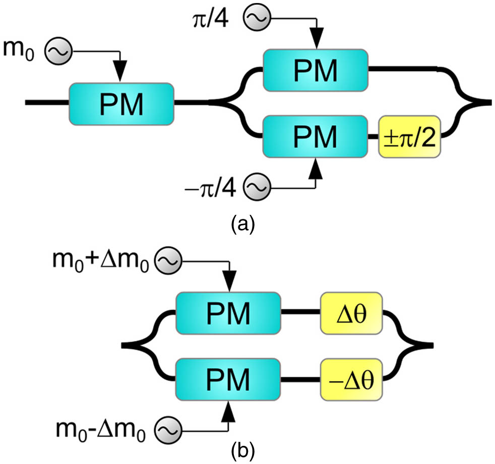
Figure 1.Schematic of (a) the PM-MZM and (b) the DD-MZM structures. Under specific phase modulation indices and static optical phase shifts, these structures produce tunable flat EO-FCs. (PM, phase modulator.)
More explicitly, let
Near
This expression is indeed the signature of a flat-top pulse train, taking a value of 1 near
B. DD-MZM Structure
The second structure for flat EO-FC generation relies on the use of a DD-MZM. Using the asymptotic formalism of the Bessel functions, it was found in Ref. [47] that, under specific imbalance driving and biasing of a DD-MZM [Fig. 1(b)], the combs produced by each PM would combine into a flat EO-FC.
Let the phase of the electric field be
Reference [47] reveals that the condition to obtain a flat comb is
To properly characterize flat EO-FCs, a common definition for the flatness is the maximum power ratio between N adjacent comb lines, in dB, noted as
3. SILICON MODULATORS
In this section, a model of a silicon plasma dispersion-based PM is introduced and compared with experimental results. This model will be used in the following to investigate the performances of the EO-FC generators.
A. Static Effects
The PM consists in a silicon waveguide, doped to form a PN junction (Fig. 2). The waveguide width is 400 nm and its height is 300 nm. It is doped with a 225 nm wide P region (targeted doping concentration:
![]()
Figure 2.Schematic cross section of the phase modulator. A PN junction is created in the waveguide to leverage the free-carrier plasma dispersion effect in the depletion regime. Higher doping concentration is used near the metallic contacts in order to reduce the access resistance. The electrical signal travels through metallic travelling wave electrodes (TWEs).
![]()
Figure 3.Variation of the effective index and propagation loss in a silicon waveguide (blue), as a function of the applied reverse voltage, compared with a linear lossless modulator example (red).
B. Dynamic Effects
The modulation length is a critical parameter for the modulation index. However, a long phase modulator (>a few millimeters) can suffer from EO-bandwidth limitations, which have to be modeled properly to evaluate the EO-FC generator properties. TWEs are usually employed as electrical access for long PMs at high frequencies (Fig. 2). Several phenomena occur by this scheme and are responsible for a limitation in the modulators’ EO bandwidth [51,52]. The impedance mismatch among the driver, TWEs, and line termination causes frequency-dependent reflections of the RF signal. The RF wave also gets attenuated along its propagation, increasingly with the frequency, due to ohmic dissipation in the doped regions of silicon and skin effect in TWEs. The mismatch between the optical and the electrical velocities causes the effective modulation to be reduced at high frequencies. Finally, the PN junction, under reverse bias, is equivalent to an electrical RC low-pass filter.
In the present numerical model, TWEs are taken into account as RF propagation lines, loaded by the PN junction, over which the electrical signal is guided in copropagation with the optical wave. For a given frequency, an electrical wave is simulated, taking account of its frequency-dependent complex propagation constant as well as reflection coefficients at the TWE input and output interfaces. An effective voltage applied to the PN junction is then calculated by integrating multiple reflections of the electrical wave, over the modulator length, and considering the optical group velocity and RF phase velocity mismatch. Finally, the RC filter transfer function is applied to the effective voltage. Employing the static model of silicon PMs, the voltage can then be converted to corresponding optical phase and intensity modulations over time. Figure 4 shows the simulated EO transfer function that is obtained for PMs of different length, embedded in one arm of a Mach–Zehnder interferometer, for a modulation frequency ranging from 0.1 to 20 GHz. The 3 dB bandwidth of a 10 mm long PM is 12.5 GHz, while it is above 20 GHz for a 2 mm long PM, showing here a limitation that is mainly due to the EO velocities mismatch.
![]()
Figure 4.Normalized simulated EO transfer function of a 10 mm (blue) and a 2 mm (red) traveling wave silicon PM, respectively, embedded in one of the arms of a Mach–Zehnder interferometer.
C. Experimental Validation
After an experimental characterization of an isolated 5 mm long silicon PM, the TWE properties are extracted, and all the aforementioned dynamic effects are implemented. To validate the numerical model, a frequency comb is simulated, considering both the dynamic and static effects. It is then compared with a frequency comb generated experimentally and measured by a heterodyne detection method described in Ref. [46]. Each comb line beats with the input laser, with an acousto-optically shifted frequency, and the beat notes are measured with a 40 GHz electrical spectrum analyzer (ESA). This technique provides a good signal-to-noise ratio and overcomes the resolution limitation of common optical spectrum analyzers. Furthermore, the beat notes’ power is proportional to the optical comb lines power. They can then be measured while scanning the modulation frequency and compared with the results from the numerical model (Fig. 5). Experimentally measured beat notes are depicted with different colors for different comb line orders, while the black curves correspond to the simulated beat notes. At a given frequency, the different line levels essentially depend on the modulation strength and nonlinearities. As the modulation frequency increases, the power of each sideband line decreases, due to the dynamic limitations of the PM. At high frequency, the effective modulation index is reduced, and the generated lines become less powerful. It can be noted that the
![]()
Figure 5.Beat notes of an EO-FC generated with an isolated 5 mm Si PM in heterodyne detection. The experimental measurements are the colored curves, where different colors correspond to different comb line orders, while the simulated beat notes are in black.
D. Silicon PMs for Flat EO-FC Generation
First, it is possible to discuss qualitatively how the nonlinear static response of silicon PMs (i.e., the nonlinear effective index variation with the applied voltage) affects the generated EO-FCs.
Figure 6(a) shows a 1 GHz sinusoidal voltage applied to a 1 cm long silicon PM, covering the full breakdown-to-forward bias range (
![]()
Figure 6.(a) 1 GHz,
In Section 2, we introduced two structures for the generation of a flat EO-FC, but the study relied on linear and lossless PMs. When implementing such structures with silicon PMs, their behavior would deviate as a consequence of the plasma-dispersion-induced nonlinearities. By referring to Fig. 6(a), it can be seen that choosing to maximize the transmission near
Indeed, finding the best operating points and driving voltages for silicon PM-MZM and DD-MZM structures is not straightforward, as compared with the case of linear lossless PMs, and a strategy is required to evaluate the best structure parameters for flat EO-FC generation.
4. FLAT FREQUENCY COMB OPTIMIZATION
In this section, a strategy to find the best operating point and driving voltage of the MZM for tunable flat EO-FC generation with both structures is given, involving the previously presented numerical model to assess the comb properties. The principle of the optimization algorithm breaks in two parts. The first part aims at flattening a comb within a
This requires first to identify what parameters will be varied to tune the comb shape, and the ones that will be fixed by design. First, all the diodes are biased with a 7 V DC reverse voltage, to which the RF component is added. To maximize the number of EO-FC lines, the modulation length and RF voltage applied to the phase shifters should be maximized. For the DD-MZM structure, the consequence is that each arm contains a 1 cm long phase shifter; the first arm is driven by a
![]()
Figure 7.Silicon (a) DD-MZM and (b) PM-MZM simulation parameters are the driving voltage
Generated EO-FC are then simulated and the N-lines flatness
The master algorithm is explained in the following: first, 16 initial couples are defined, with four values for
5. RESULTS AND BANDWIDTH SCALING
Figure 8 shows the obtained
![]()
Figure 8.Optimum driving voltage peak-to-peak amplitude
Figure 8(c) shows a 2 dB flatness can be achieved in the whole frequency range with both structures. A mean conversion efficiency between
In Fig. 9, the widest achievable EO-FCs at specific line spacings of 2, 6, and 10 GHz are displayed for both structures, exhibiting similar shapes. The best number of lines in a 2 dB flatness range is shown in Fig. 9(g), as a function of the modulation frequency. A flat comb with at least nine lines is obtained up to 7 GHz. The line-spacing tunability limitation comes from the modulator’s bandwidth in both structures: a 1 cm long PM has a 12.5 GHz EO BW, as simulated in Section 3 (Fig. 4). Because the PMs are long, the EO velocity mismatch limits the induced modulation index and, thus, the number of flat lines, as the modulation frequency increases. To overcome this issue, one solution is to divide the PMs in multiple sections, as shown in Fig. 10(a), and to feed each section with a finely delayed replica of the driving signal. This technique reduces the influence from the velocity mismatch and the electrical propagation loss limitations. To show the benefits of segmenting the PMs, the optimal flat combs were simulated for the DD-MZM structure, with its 1 cm PMs being segmented into M elements of 1/M cm. For each configuration, the applied voltage and phase shifts were optimized using the algorithm detailed in Section 4. The resulting line number within the 2 dB criterion is plotted in Fig. 10(b) for M going from 1 to 5, showing a strong improvement in terms of line spacing tunability, with segmented PMs. By splitting the 1 cm PM into five elements of 2 mm, a flat EO-FC with at least nine lines can be obtained with up to 39 GHz line spacing, competing with the current widest flat EO-FCs in the silicon platform [16,17,45].
![]()
Figure 9.Optimum flat EO-FCs obtained with the DD-MZM at (a) 2 GHz, (b) 6 GHz, (c) 10 GHz and with the PM-MZM structure at (d) 2 GHz, (e) 6 GHz, and (f) 10 GHz. (g) Best achievable number of comb lines in a 2 dB flatness over the 15 GHz modulation frequency range with both structures.
![]()
Figure 10.(a) DD-MZM with segmented PMs. Each arm contains
6. CONCLUSION
Silicon modulators are a technology of choice for the integration of photonics circuits. In this article, their suitability for flat EO-FC generation was investigated. After detailing the operation principle of a PM-MZM and a DD-MZM structures for this purpose, a numerical model of a silicon traveling wave PM was presented and used to evaluate the performance of silicon PMs for EO-FC generation. An algorithm was implemented to optimize the driving electrical power and static optical phase shifts in both structures. As a result, it was found that a flat EO-FC containing nine lines can be generated, with a line spacing being freely tunable from 0.1 to 7 GHz with both structures. It was also shown that, by segmenting the PMs, the tunability of a silicon-modulator-based EO-FC can be strongly improved. With five segments of 2 mm long PMs in each arm of a DD-MZM, the simulation shows that a flat EO-FC with nine lines can be tuned up to a 39 GHz line spacing. These performances could be beneficial for on-chip dual-comb or RF photonics applications, where the line-spacing tunability can be advantageous.
Acknowledgment
Acknowledgment. Diego Perez-Galacho acknowledges the support of the Spanish Ministry of Science, Innovation and Universities through the Juan de la Cierva fellowship program.
References
[1] S. A. Diddams, K. Vahala, T. Udem. Optical frequency combs: coherently uniting the electromagnetic spectrum. Science, 369, eaay3676(2020).
[2] T. Udem, R. Holzwarth, T. W. Hänsch. Optical frequency metrology. Nature, 416, 233-237(2002).
[3] S. A. Diddams, D. J. Jones, L.-S. Ma, S. T. Cundiff, J. L. Hall. Optical frequency measurement across a 104-THz gap with a femtosecond laser frequency comb. Opt. Lett., 25, 186-188(2000).
[4] M. Kourogi, K. Nakagawa, M. Ohtsu. Wide-span optical frequency comb generator for accurate optical frequency difference measurement. IEEE J. Quantum Electron., 29, 2693-2701(1993).
[5] V. Torres-Company, J. Schroder, A. Fulop, M. Mazur, L. Lundberg, O. B. Helgason, M. Karlsson, P. A. Andrekson. Laser frequency combs for coherent optical communications. J. Lightwave Technol., 37, 1663-1670(2019).
[6] I. Coddington, N. Newbury, W. Swann. Dual-comb spectroscopy. Optica, 3, 414-426(2016).
[7] N. Picqué, T. W. Hänsch. Frequency comb spectroscopy. Nat. Photonics, 13, 146-157(2019).
[8] N. Kuse, M. E. Fermann. Frequency-modulated comb LIDAR. APL Photon., 4, 106105(2019).
[9] V. Torres-Company, A. M. Weiner. Optical frequency comb technology for ultrabroadband radiofrequency photonics. Laser Photon. Rev., 8, 368-393(2013).
[10] M. S. Alshaykh, J. D. McKinney, A. M. Weiner. Radio-frequency signal processing using optical frequency combs. IEEE Photon. Technol. Lett., 31, 1874-1877(2019).
[11] C. Deakin, Z. Liu. Noise and distortion analysis of dual frequency comb photonic RF channelizers. Opt. Express, 28, 39750-39769(2020).
[12] J. Feldmann, N. Youngblood, M. Karpov, H. Gehring, X. Li, M. Stappers, M. L. Gallo, X. Fu, A. Lukashchuk, A. S. Raja, J. Liu, C. D. Wright, A. Sebastian, T. J. Kippenberg, W. H. P. Pernice, H. Bhaskaran. Parallel convolution processing using an integrated photonic tensor core. Nature, 589, 52-58(2021).
[13] B. J. Shastri, A. N. Tait, T. Ferreira de Lima, W. H. P. Pernice, H. Bhaskaran, C. D. Wright, P. R. Prucnal. Photonics for artificial intelligence and neuromorphic computing. Nat. Photonics, 15, 102-114(2021).
[14] A. Parriaux, K. Hammani, G. Millot. Electro-optic frequency combs. Adv. Opt. Photon., 12, 223-287(2020).
[15] F. Bontempi, N. Andriolli, F. Scotti, M. Chiesa, G. Contestabile. Comb line multiplication in an InP integrated photonic circuit based on cascaded modulators. IEEE J. Sel. Top. Quantum Electron., 25, 3500107(2019).
[16] S. Liu, K. Wu, L. Zhou, L. Lu, B. Zhang, G. Zhou, J. Chen. Optical frequency comb and Nyquist pulse generation with integrated silicon modulators. IEEE J. Sel. Top. Quantum Electron., 26, 8300208(2020).
[17] Z. Wang, M. Ma, H. Sun, M. Khalil, R. Adams, K. Yim, X. Jin, L. R. Chen. Optical frequency comb generation using CMOS compatible cascaded Mach–Zehnder modulators. IEEE J. Quantum Electron., 55, 8400206(2019).
[18] I. Demirtzioglou, C. Lacava, K. R. H. Bottrill, D. J. Thomson, G. T. Reed, D. J. Richardson, P. Petropoulos. Frequency comb generation in a silicon ring resonator modulator. Opt. Express, 26, 790-797(2018).
[19] J. Lin, H. Sepehrian, W. Shi. Frequency comb generation using a CMOS compatible SiP DD-MZM for flexible networks. IEEE Photon. Technol. Lett., 30, 1495-1498(2018).
[20] J. Qian, S. Tian, L. Shang. Investigation on Nyquist pulse generation by optical frequency comb. J. Opt. Technol., 83, 699-702(2016).
[21] A. K. Mishra, R. Schmogrow, I. Tomkos, D. Hillerkuss, C. Koos, W. Freude, J. Leuthold. Flexible RF-based comb generator. IEEE Photon. Technol. Lett., 25, 701-704(2013).
[22] M. Khalil, R. Maram, B. Naghdi, A. Samani, M. Jacques, L. R. Chen, D. V. Plant. Electro-optic frequency comb generation using cascaded silicon microring modulators. OSA Advanced Photonics Congress, IM3A.6(2020).
[23] K. P. Nagarjun, V. Jeyaselvan, S. K. Selvaraja, V. R. Supradeepa. Generation of tunable, high repetition rate optical frequency combs using on-chip silicon modulators. Opt. Express, 26, 10744-10753(2018).
[24] X. Wu, H. K. Tsang. Flat-top frequency comb generation with silicon microring modulator and filter. Conference on Lasers and Electro-Optics, SM4O.6(2017).
[25] A. Parriaux, M. Conforti, A. Bendahmane, J. Fatome, C. Finot, S. Trillo, N. Picqué, G. Millot. Spectral broadening of picosecond pulses forming dispersive shock waves in optical fibers. Opt. Lett., 42, 3044-3047(2017).
[26] G. Millot, S. Pitois, M. Yan, T. Hovhannisyan, A. Bendahmane, T. W. Hänsch, N. Picqué. Frequency-agile dual-comb spectroscopy. Nat. Photonics, 10, 27-30(2016).
[27] R. Wu, V. Torres-Company, D. E. Leaird, A. M. Weiner. Supercontinuum-based 10-GHz flat-topped optical frequency comb generation. Opt. Express, 21, 6045-6052(2013).
[28] V. Torres-Company, J. Lancis, P. Andrés. Lossless equalization of frequency combs. Opt. Lett., 33, 1822-1824(2008).
[29] H.-J. Kim, A. J. Metcalf, O. E. Sandoval, D. E. Leaird, A. M. Weiner. Broadband and ultra-flat optical comb generation using an EO comb source and a programmable pulse shaper. Conference on Lasers and Electro-Optics (CLEO), JW2A.72(2014).
[30] A. J. Metcalf, V. Torres-Company, D. E. Leaird, A. M. Weiner. High-power broadly tunable electrooptic frequency comb generator. IEEE J. Quantum Electron., 19, 3500306(2013).
[31] R. Wu, V. R. Supradeepa, C. M. Long, D. E. Leaird, A. M. Weiner. Generation of very flat optical frequency combs from continuous-wave lasers using cascaded intensity and phase modulators driven by tailored radio frequency waveforms. Opt. Lett., 35, 3234-3236(2010).
[32] T. Sakamoto, A. Chiba. Multiple-frequency-spaced flat optical comb generation using a multiple-parallel phase modulator. Opt. Lett., 42, 4462-4465(2017).
[33] N. Yokota, H. Yasaka. Operation strategy of InP Mach–Zehnder modulators for flat optical frequency comb generation. IEEE J. Quantum Electron., 52, 5200207(2016).
[34] R. Slavik, S. G. Farwell, M. J. Wale, D. J. Richardson. Compact optical comb generator using InP tunable laser and push-pull modulator. IEEE Photon. Technol. Lett., 27, 217-220(2015).
[35] C. Weimann, P. C. Schindler, R. Palmer, S. Wolf, D. Bekele, D. Korn, J. Pfeifle, S. Koeber, R. Schmogrow, L. Alloatti, D. Elder, H. Yu, W. Bogaerts, L. R. Dalton, W. Freude, J. Leuthold, C. Koos. Silicon-organic hybrid (SOH) frequency comb sources for terabit/s data transmission. Opt. Express, 22, 3629-3637(2014).
[36] T. Sakamoto, T. Kawanishi, M. Tsuchiya. 10 GHz, 24 ps pulse generation using a single-stage dual-drive Mach-Zehnder modulator. Opt. Lett., 33, 890-892(2008).
[37] K. Li, S. Liu, D. J. Thomson, W. Zhang, X. Yan, F. Meng, C. G. Littlejohns, H. Du, M. Banakar, M. Ebert, W. Cao, D. Tran, B. Chen, A. Shakoor, P. Petropoulos, G. T. Reed. Electronic–photonic convergence for silicon photonics transmitters beyond 100 Gbps on–off keying. Optica, 7, 1514-1516(2020).
[38] X. Chen, M. M. Milosevic, A. F. J. Runge, X. Yu, A. Z. Khokhar, S. Mailis, D. J. Thomson, A. C. Peacock, S. Saito, G. T. Reed. Silicon erasable waveguides and directional couplers by germanium ion implantation for configurable photonic circuits. Opt. Express, 28, 17630-17642(2020).
[39] G. Zhou, Y. Guo, L. Lu, J. Chen, L. Zhou. Ultra-wideband signal generation based on a silicon segmented Mach-Zehnder modulator. IEEE Photon. J., 12, 5502615(2020).
[40] D. Marris-Morini, C. Baudot, J.-M. Fédéli, G. Rasigade, N. Vulliet, A. Souhaité, M. Ziebell, P. Rivallin, S. Olivier, P. Crozat, X. L. Roux, D. Bouville, S. Menezo, F. Bœuf, L. Vivien. Low loss 40 Gbit/s silicon modulator based on interleaved junctions and fabricated on 300 mm SOI wafers. Opt. Express, 21, 22471-22475(2013).
[41] A. Samani, D. Patel, M. Chagnon, E. El-Fiky, R. Li, M. Jacques, N. Abadía, V. Veerasubramanian, D. V. Plant. Experimental parametric study of 128 Gb/s PAM-4 transmission system using a multi-electrode silicon photonic Mach Zehnder modulator. Opt. Express, 25, 13252-13262(2017).
[42] M. H. Idjadi, S. Arab, F. Aflatouni. Optical frequency comb generation in silicon by recursive electro-optic modulation. Conference on Lasers and Electro-Optics, SF3O.5(2020).
[43] K. P. Nagarjun, P. Raj, V. Jeyaselvan, S. K. Selvaraja, V. R. Supradeepa. Microwave power induced resonance shifting of silicon ring modulators for continuously tunable, bandwidth scaled frequency combs. Opt. Express, 28, 13032-13042(2020).
[44] Y. Xu, J. Lin, R. Dubé-Demers, S. LaRochelle, L. Rusch, W. Shi. Integrated flexible-grid WDM transmitter using an optical frequency comb in microring modulators. Opt. Lett., 43, 1554-1557(2018).
[45] K. P. Nagarjun, R. Prakash, B. S. Vikram, S. Arora, V. Jeyaselvan, S. K. Selvaraja, V. R. Supradeepa. Bandwidth scaling of silicon modulator-based combs using multi-carriers and frequency offset locking. OSA Contin., 3, 921-928(2020).
[46] L. Deniel, E. Weckenmann, D. P. Galacho, C. Alonso-Ramos, F. Boeuf, L. Vivien, D. Marris-Morini. Frequency-tuning dual-comb spectroscopy using silicon Mach-Zehnder modulators. Opt. Express, 28, 10888-10898(2020).
[47] T. Sakamoto, T. Kawanishi, M. Izutsu. Asymptotic formalism for ultraflat optical frequency comb generation using a Mach-Zehnder modulator. Opt. Lett., 32, 1515-1517(2007).
[48] H. Murata, A. Morimoto, T. Kobayashi, S. Yamamoto. Optical pulse generation by electrooptic-modulation method and its application to integrated ultrashort pulse generators. IEEE J. Sel. Top. Quantum Electron., 6, 1325-1331(2000).
[49] R. Soref, B. Bennett. Electrooptical effects in silicon. IEEE J. Quantum Electron., 23, 123-129(1987).
[50] C. Baudot, A. Fincato, D. Fowler, D. Perez-Galacho, A. Souhaité, S. Messaoudène, R. Blanc, C. Richard, J. Planchot, C. De-Buttet, B. Orlando, F. Gays, C. Mezzomo, E. Bernard, D. Marris-Morini, L. Vivien, C. Kopp, F. Boeuf. DAPHNE silicon photonics technological platform for research and development on WDM applications. Proc. SPIE, 9891, 98911D(2016).
[51] J. Witzens. High-speed silicon photonics modulators. Proc. IEEE, 106, 2158-2182(2018).
[52] A. Samani, E. El-Fiky, M. Morsy-Osman, R. Li, D. Patel, T. Hoang, M. Jacques, M. Chagnon, N. Abadia, D. V. Plant. Silicon photonic Mach–Zehnder modulator architectures for on chip PAM-4 signal generation. J. Lightwave Technol., 37, 2989-2999(2019).


Set citation alerts for the article
Please enter your email address

© Copyright 2018-2021 | Chinese Laser Press. All Rights Reserved 沪ICP备15018463号-20