• Photonics Research
  • Vol. 9, Issue 4, 471 (2021)
Omid Jafari1、*, Sasan Zhalehpour2, Wei Shi1, and Sophie LaRochelle1
Author Affiliations
  • 1Centre d’optique, photonique et laser (COPL), Université Laval, Québec City, Québec, Canada
  • 2Canada Research Center, Huawei Technologies Canada, Ottawa, Ontario, Canada
  • show less
    DOI: 10.1364/PRJ.414400 Cite this Article Set citation alerts
    Omid Jafari, Sasan Zhalehpour, Wei Shi, Sophie LaRochelle. Mode-conversion-based silicon photonic modulator loaded by a combination of lateral and interleaved p-n junctions[J]. Photonics Research, 2021, 9(4): 471 Copy Citation Text show less
    Schematic of (a) the full modulator structure, (b) the asymmetric directional coupler, (c) the taper between the asymmetric directional coupler and the asymmetric Bragg structure, and (d) the asymmetric Bragg grating waveguide loaded by a C-LI p-n junction and its cross section. The parameter values are in micrometers.
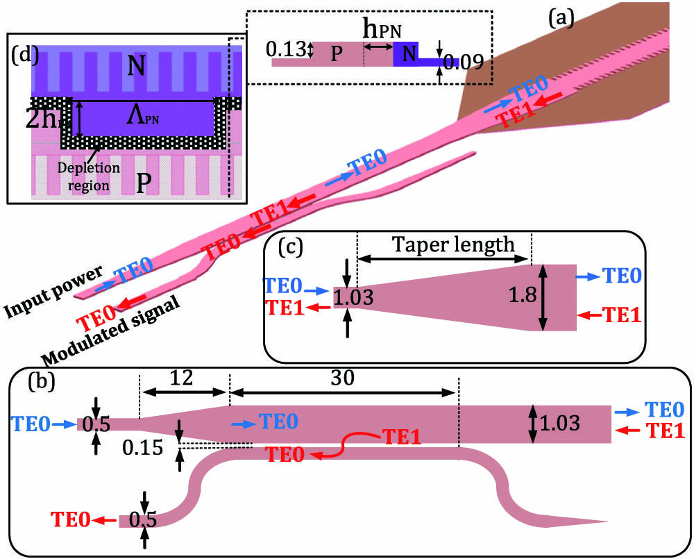
    Fig. 1. Schematic of (a) the full modulator structure, (b) the asymmetric directional coupler, (c) the taper between the asymmetric directional coupler and the asymmetric Bragg structure, and (d) the asymmetric Bragg grating waveguide loaded by a C-LI p-n junction and its cross section. The parameter values are in micrometers.
    Spectral response of the asymmetric directional coupler simulated in Lumerical-FDTD showing the transmission of the input TE0 mode to the through port (blue) and the transmission of the reflected TE1 mode to the drop port (red).
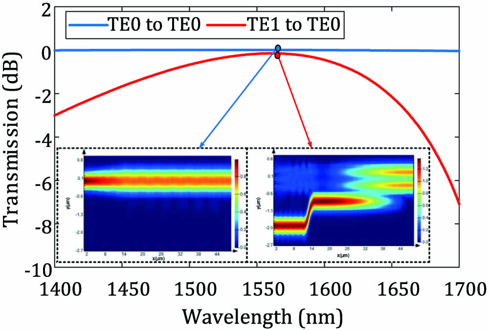
    Fig. 2. Spectral response of the asymmetric directional coupler simulated in Lumerical-FDTD showing the transmission of the input TE0 mode to the through port (blue) and the transmission of the reflected TE1 mode to the drop port (red).
    Schematic of (a) lateral, (b) interleaved, and (c) C-LI p-n junctions; (d) refractive index variations for TE0 and TE1 modes, and the Bragg wavelength shift as a function of the PN junction offset at a reverse bias of 2 V for lateral p-n junctions; (e) sum of refractive index modulation for TE0 and TE1 modes (Δn0+Δn1) as a function of reverse bias for different p-n junction profiles.
    Fig. 3. Schematic of (a) lateral, (b) interleaved, and (c) C-LI p-n junctions; (d) refractive index variations for TE0 and TE1 modes, and the Bragg wavelength shift as a function of the PN junction offset at a reverse bias of 2 V for lateral p-n junctions; (e) sum of refractive index modulation for TE0 and TE1 modes (Δn0+Δn1) as a function of reverse bias for different p-n junction profiles.
    Refractive index variations for TE0 (blue line) and TE1 (red line) modes as well as sum of them (Δn0+Δn1) as a function of junction offset.
    Fig. 4. Refractive index variations for TE0 (blue line) and TE1 (red line) modes as well as sum of them (Δn0+Δn1) as a function of junction offset.
    SEM picture of (a) the directional coupler, and (b) the asymmetric Bragg grating waveguide.
    Fig. 5. SEM picture of (a) the directional coupler, and (b) the asymmetric Bragg grating waveguide.
    Measured spectra of the asymmetric directional coupler when (a) the power is input in Port 1 and coupled to the TE0 mode in the multimode waveguide, and (b) the power is input in Port 4 and coupled to the TE1 mode in the multimode waveguide.
    Fig. 6. Measured spectra of the asymmetric directional coupler when (a) the power is input in Port 1 and coupled to the TE0 mode in the multimode waveguide, and (b) the power is input in Port 4 and coupled to the TE1 mode in the multimode waveguide.
    Phase shift of asymmetric Bragg grating modulators with different p-n junction profiles as a function of the reverse voltage.
    Fig. 7. Phase shift of asymmetric Bragg grating modulators with different p-n junction profiles as a function of the reverse voltage.
    Zoom in on the edge of the optical spectra, where the modulator is operated, of the asymmetric Bragg grating waveguide for reverse bias voltages of 0 and 2 V.
    Fig. 8. Zoom in on the edge of the optical spectra, where the modulator is operated, of the asymmetric Bragg grating waveguide for reverse bias voltages of 0 and 2 V.
    Small-signal measurement of the asymmetric Bragg grating modulator for different reverse voltages.
    Fig. 9. Small-signal measurement of the asymmetric Bragg grating modulator for different reverse voltages.
    Block diagram of the experimental setup.
    Fig. 10. Block diagram of the experimental setup.
    BER as a function of the received power for different modulation speeds.
    Fig. 11. BER as a function of the received power for different modulation speeds.
    (a) Measured BER as a function of bitrate without and with applying DD-MMSE equalizer; histograms of detected bits (one sample per symbol) used for BER calculation at bitrates of (b) 45 Gb/s and (c) 55 Gb/s. The dashed lines show the Gaussian distributions in (b) and (c).
    Fig. 12. (a) Measured BER as a function of bitrate without and with applying DD-MMSE equalizer; histograms of detected bits (one sample per symbol) used for BER calculation at bitrates of (b) 45 Gb/s and (c) 55 Gb/s. The dashed lines show the Gaussian distributions in (b) and (c).
    Omid Jafari, Sasan Zhalehpour, Wei Shi, Sophie LaRochelle. Mode-conversion-based silicon photonic modulator loaded by a combination of lateral and interleaved p-n junctions[J]. Photonics Research, 2021, 9(4): 471
    Download Citation