
Omid Jafari, Sasan Zhalehpour, Wei Shi, Sophie LaRochelle, "Mode-conversion-based silicon photonic modulator loaded by a combination of lateral and interleaved p-n junctions," Photonics Res. 9, 471 (2021)
- Photonics Research
- Vol. 9, Issue 4, 471 (2021)
Abstract
1. INTRODUCTION
Photonic integration leverages design kits of silicon photonic (SiP) components to achieve high yield and reduced costs using the mature complementary metal oxide-semiconductor (CMOS) manufacturing process. A key element of integrated transceivers is SiP modulators, which have received considerable attention during the last decade. SiP Mach–Zehnder modulators (MZMs) and microring modulators (MRMs) have thus been demonstrated with high-speed operation and high stability in the former case, and low energy per bit with an ultracompact footprint in the latter case [1–4]. Despite these attractive properties, the narrow optical bandwidth of MRMs makes them difficult to stabilize, while the long phase shifter MZMs are energy-hungry. Bragg grating modulators, through careful optimization of their structure, offer the potential to improve this performance trade-off, i.e., offering a compact solution with reduced stabilization requirements [5–7].
Analysis of Bragg grating modulators shows that operating the device in the reflection is more efficient than using it in transmission [8]. More specifically, when operated in reflection, the grating strength can be lower for a given optical modulation amplitude, thereby introducing less time delay and improving modulation speed [8]. However, operation in reflection is typically characterized by higher loss due to the lack of on-chip circulators. Therefore, the signal from Bragg grating modulators operated in reflection is typically retrieved by either an external circulator, adding complexity and cost, or by an on-chip splitter, e.g., a Y-junction that introduces an additional loss of 6 dB.
In Ref. [9], we proposed using asymmetric Bragg gratings to achieve modulation in reflection with low on-chip loss and without the need for circulators. The mode conversion introduced by the asymmetric Bragg grating allows one to direct the reflected signal to a drop port with low loss. In our initial work, we used an asymmetric Y-branch to filter the reflected mode, and phase modulation was achieved by a standard lateral p-n junction [10]. In this work, to optimize the phase modulation, we introduce a novel design of an asymmetric Bragg grating modulator loaded with a combination of lateral and interleaved (C-LI) p-n junctions. We experimentally show that the C-LI p-n junction increases the phase modulation by 67%, compared to the lateral p-n junction, with design features that respect the requirements of standard fabrication processes. We further propose an asymmetric directional coupler, instead of an asymmetric Y-branch, to reduce insertion loss and cross talk. This optimized design, with a phase shifter length of 290 μm, demonstrates modulation speeds up to 55 Gb/s, with an estimated power consumption of 226 fJ/bit.
Sign up for Photonics Research TOC. Get the latest issue of Photonics Research delivered right to you!Sign up now
2. DESIGN AND MODULATOR STRUCTURE
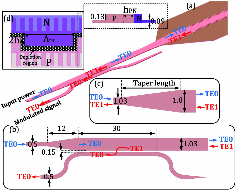
Figure 1.Schematic of (a) the full modulator structure, (b) the asymmetric directional coupler, (c) the taper between the asymmetric directional coupler and the asymmetric Bragg structure, and (d) the asymmetric Bragg grating waveguide loaded by a C-LI p-n junction and its cross section. The parameter values are in micrometers.
A. Asymmetric Directional Coupler
![]()
Figure 2.Spectral response of the asymmetric directional coupler simulated in Lumerical-FDTD showing the transmission of the input TE0 mode to the through port (blue) and the transmission of the reflected TE1 mode to the drop port (red).
Finally, note that a taper, shown in Fig. 1(c), is placed between the directional coupler multimode output and the multimode waveguide with the asymmetric Bragg grating in order to insure mode-matching. Simulations showed that a taper length of at least 10 μm was required to guarantee low loss for both modes. We chose a 20 μm taper length.
B. Asymmetric Bragg Grating Waveguide
The asymmetric Bragg grating consists of a waveguide whose sidewall gratings are placed with a
![]()
Figure 3.Schematic of (a) lateral, (b) interleaved, and (c) C-LI p-n junctions; (d) refractive index variations for TE0 and TE1 modes, and the Bragg wavelength shift as a function of the PN junction offset at a reverse bias of 2 V for lateral p-n junctions; (e) sum of refractive index modulation for TE0 and TE1 modes (
![]()
Figure 4.Refractive index variations for TE0 (blue line) and TE1 (red line) modes as well as sum of them (
3. DEVICE CHARACTERIZATION
![]()
Figure 5.SEM picture of (a) the directional coupler, and (b) the asymmetric Bragg grating waveguide.
A. Asymmetric Directional Coupler
![]()
Figure 6.Measured spectra of the asymmetric directional coupler when (a) the power is input in Port 1 and coupled to the TE0 mode in the multimode waveguide, and (b) the power is input in Port 4 and coupled to the TE1 mode in the multimode waveguide.
Compared to the asymmetric Y-branch reported in Ref. [10], the directional coupler has a broader spectral response, lower loss over the C-band, and significantly less cross talk. The asymmetric Y-branch was characterized by an operating bandwidth of 15 nm, an insertion loss of 1.5 dB, and a cross talk of 7 dB, while the directional coupler improves these parameters to 35 nm, 1 dB, and 30 dB, respectively.
B. Modulator Characterization
![]()
Figure 7.Phase shift of asymmetric Bragg grating modulators with different p-n junction profiles as a function of the reverse voltage.
![]()
Figure 8.Zoom in on the edge of the optical spectra, where the modulator is operated, of the asymmetric Bragg grating waveguide for reverse bias voltages of 0 and 2 V.
![]()
Figure 9.Small-signal measurement of the asymmetric Bragg grating modulator for different reverse voltages.
![]()
Figure 10.Block diagram of the experimental setup.
![]()
Figure 11.BER as a function of the received power for different modulation speeds.
![]()
Figure 12.(a) Measured BER as a function of bitrate without and with applying DD-MMSE equalizer; histograms of detected bits (one sample per symbol) used for BER calculation at bitrates of (b) 45 Gb/s and (c) 55 Gb/s. The dashed lines show the Gaussian distributions in (b) and (c).
4. CONCLUSION
We presented a mode-conversion-based SiP modulator that takes advantage of lateral and interleaved p-n junctions simultaneously to enhance phase modulation. The modulator gains a 67% improvement in the phase modulation when loaded by the C-LI p-n junction compared to the lateral one. We employed an asymmetric Bragg grating waveguide to convert the incident TE0 mode to a reflected TE1 mode in order to direct the modulated signal to a drop port by using an asymmetric directional coupler. The whole structure therefore acts similarly to an on-chip circulator and avoids the usually high insertion loss of Bragg grating modulators. The experimentally demonstrated modulator had a phase shifter length of 290 μm, an insertion loss of 2 dB, and power consumption of 226 fJ/bit. The modulator operated up to 45 Gb/s (55 Gb/s) with BER below the 7% (20%) FEC threshold, showing a great potential for high-speed, low-cost, power-efficient transmissions.
Acknowledgment
Acknowledgment. The authors thank CMC Microsystems for the fabrication subsidy and MPW service.
References
[10] O. Jafari, J. Lin, W. Shi, S. LaRochelle. Mode-conversion-based silicon photonic modulator using asymmetric Bragg grating and Y-branch. European Conference on Optical Communication, 1-2(2019).


Set citation alerts for the article
Please enter your email address

© Copyright 2018-2021 | Chinese Laser Press. All Rights Reserved 沪ICP备15018463号-20