• Infrared and Laser Engineering
  • Vol. 51, Issue 3, 20220043 (2022)
Qi He1、2, Yaru Wang1、2, Weicheng Chen1、2, Dian Wan1、2, Si Chen3, Haoran Gao1、2, Rongxiang Guo1、2, Yisheng Gao1、2, Jiaqi Wang4、*, Zhenzhou Cheng1、2, Yu Yu5、*, and Tiegen Liu1、2
Author Affiliations
  • 1School of Precision Instrument and Opto-Electronics Engineering, Tianjin University, Tianjin 300072, China
  • 2Key Laboratory of Opto-Electronics Information Technology, Ministry of Education, Tianjin 300072, China
  • 3College of Physics and Optoelectronics, Taiyuan University of Technology, Taiyuan 030024, China
  • 4College of Physics and Optoelectronic Engineering, Shenzhen University, Shenzhen 518060, China
  • 5Wuhan National Laboratory for Optoelectronics, Huazhong University of Science and Technology, Wuhan 430074, China
  • show less
    DOI: 10.3788/IRLA20220043 Cite this Article
    Qi He, Yaru Wang, Weicheng Chen, Dian Wan, Si Chen, Haoran Gao, Rongxiang Guo, Yisheng Gao, Jiaqi Wang, Zhenzhou Cheng, Yu Yu, Tiegen Liu. Advances in short-wavelength mid-infrared silicon photonics (Invited)[J]. Infrared and Laser Engineering, 2022, 51(3): 20220043 Copy Citation Text show less
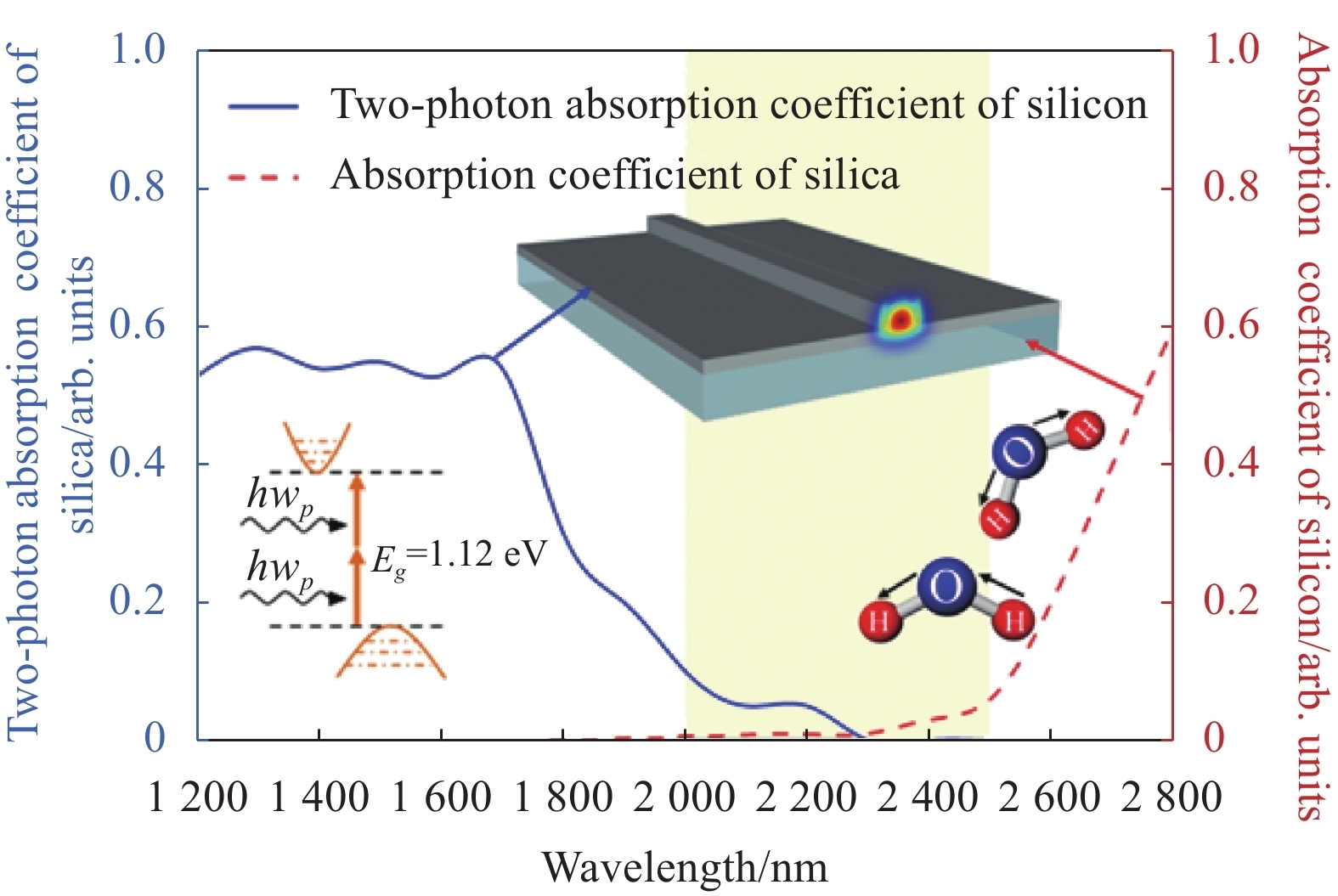
    Silicon waveguide devices based on SOI have low two-photon absorption and low BOX absorption in the short-wavelength mid-IR band[22, 25-26]
    Fig. 1. Silicon waveguide devices based on SOI have low two-photon absorption and low BOX absorption in the short-wavelength mid-IR band[22, 25-26]
    Silicon waveguides in the short-wavelength mid-IR band. (a) Measurement result of optical loss of the TE0-mode strip (left) and rib (right) silicon waveguides[42]; (b) Scanning electron microscope (SEM) images of the silicon waveguide fabricated with the MPW service[27]; (c) SEM image of the SMW cross section[44]; (d) Schematic of the subwavelength-grating-cladding suspended slot waveguide[45]
    Fig. 2. Silicon waveguides in the short-wavelength mid-IR band. (a) Measurement result of optical loss of the TE0-mode strip (left) and rib (right) silicon waveguides[42]; (b) Scanning electron microscope (SEM) images of the silicon waveguide fabricated with the MPW service[27]; (c) SEM image of the SMW cross section[44]; (d) Schematic of the subwavelength-grating-cladding suspended slot waveguide[45]
    Silicon grating couplers in the short-wavelength mid-IR band. (a) SEM image of the shallow-etched uniform grating coupler[53]; (b) Schematic of the polysilicon/silicon grating coupler[40]; (c) SEM image of the focusing subwavelength grating coupler fabricated with the MPW service[27]; (d) Measurement results of the ultra-thin focusing subwavelength grating coupler[55]
    Fig. 3. Silicon grating couplers in the short-wavelength mid-IR band. (a) SEM image of the shallow-etched uniform grating coupler[53]; (b) Schematic of the polysilicon/silicon grating coupler[40]; (c) SEM image of the focusing subwavelength grating coupler fabricated with the MPW service[27]; (d) Measurement results of the ultra-thin focusing subwavelength grating coupler[55]
    Silicon micro-resonators in the short-wavelength mid-IR band. (a) SEM image of the racetrack microring resonator[60]; (b) Schematic picture of the suspended membrane ring resonator[44]; (c) Microscope image of the tunable microring resonator[61]; (d) SEM image of the microdisk resonator with the subwavelength grating structure[63]
    Fig. 4. Silicon micro-resonators in the short-wavelength mid-IR band. (a) SEM image of the racetrack microring resonator[60]; (b) Schematic picture of the suspended membrane ring resonator[44]; (c) Microscope image of the tunable microring resonator[61]; (d) SEM image of the microdisk resonator with the subwavelength grating structure[63]
    Silicon multiplexing/demultiplexing devices in the short-wavelength mid-IR band. (a) The transmission spectrum image of different channels (left) and microscope image (right) of the AWG[69]; (b) Microscope image of the echelle grating[68]; (c) Schematic of the silicon multi-mode multiplexing/demultiplexing devices[71]; (d) Measured bit error rate (BER) of the silicon multi-mode multiplexing/demultiplexing devices as a function of the received optical signal-to-noise ratio (OSNR)[71]
    Fig. 5. Silicon multiplexing/demultiplexing devices in the short-wavelength mid-IR band. (a) The transmission spectrum image of different channels (left) and microscope image (right) of the AWG[69]; (b) Microscope image of the echelle grating[68]; (c) Schematic of the silicon multi-mode multiplexing/demultiplexing devices[71]; (d) Measured bit error rate (BER) of the silicon multi-mode multiplexing/demultiplexing devices as a function of the received optical signal-to-noise ratio (OSNR)[71]
    Nonlinear optical waveguide devices in the short-wavelength mid-IR band. (a) Wavelength conversion across more than one octave based on FWM[74]; (b) SCG based on the SOI waveguide[77]; (c) Schematic of the Kerr frequency comb generation in the microring resonator[82]; (d) Spectrum and intracavity power of the KFC based on the Si/Ge waveguide[82]
    Fig. 6. Nonlinear optical waveguide devices in the short-wavelength mid-IR band. (a) Wavelength conversion across more than one octave based on FWM[74]; (b) SCG based on the SOI waveguide[77]; (c) Schematic of the Kerr frequency comb generation in the microring resonator[82]; (d) Spectrum and intracavity power of the KFC based on the Si/Ge waveguide[82]
    Optoelectronic waveguide devices in the short-wavelength mid-IR band. (a) Cross-sectional schematic diagram of the active region of the p-i-n diode phase-shifter[83]; (b) Optical microscope image of the MZM [84]; (c) Schematic of the racetrack microring resonator-enhanced WSi nanowire photodetector. The red line indicates the waveguide on which the WSi nanowire is integrated[91]; (d) SEM image of the cross-section of the Zn2+-implanted Si waveguide photodiodes [92]
    Fig. 7. Optoelectronic waveguide devices in the short-wavelength mid-IR band. (a) Cross-sectional schematic diagram of the active region of the p-i-n diode phase-shifter[83]; (b) Optical microscope image of the MZM [84]; (c) Schematic of the racetrack microring resonator-enhanced WSi nanowire photodetector. The red line indicates the waveguide on which the WSi nanowire is integrated[91]; (d) SEM image of the cross-section of the Zn2+-implanted Si waveguide photodiodes [92]
    No.WaferWavelength/ μm Optical loss/ dB·cm−1Waveguide typeRef.
    1SOI2.20.6Strip[40]
    2SOI21.00±0.008Rib[41]
    3SOS2.081.4Strip[43]
    4SOI2.021.9±0.2Rib[42]
    5SOI2.023.3±0.5Strip[42]
    6SOI2.257.9Suspended slot[45]
    Table 1. Characteristics of the silicon waveguides in the short-wavelength mid-IR band
    No.WaferEtch depth /nm StructureWavelength/μmBandwidth /nm Efficiency /dB Ref.
    1SOI70SEGC2.15160 (3 dB)−5.2[53]
    2SOI240SEGC2.190 (3 dB)−3.8[40]
    3SOIN/AFSGC2.255/2.33138/54 (1 dB)−5.9/−5.7[54]
    4SOI70FSGC2.3685 (3 dB)−7.77[27]
    5SOI150FSGC2.2115 (1 dB)−7.1[55]
    Table 2. Characteristics of the silicon grating couplers in the short-wavelength mid-IR band
    No.WaferQ factor FSR /nm StructureRef.
    1SOI750003.9Microring[24]
    2SOI170004.5Microring[5]
    3SOS11400N/ARacetrack microring[60]
    4SOI110004.47Microring with p-type doping[5]
    5SOI8100N/ASuspended membrane microring[44]
    6SOI152012Racetrack microring[61]
    7SOI80040Subwavelength grating microdisk[63]
    Table 3. Characteristics of the silicon micro-resonators in the short-wavelength mid-IR band
    No.Wavelength /μm Insertion loss /dB Crosstalk /dB StructureRef.
    126−15.7AWG[69]
    22.1/2.3High< −16EG[68]
    32.24−16AWG[68]
    42< 5< −18DC[71]
    521.2−18.83MMI[70]
    Table 4. Characteristics of the silicon multiplexing/demultiplexing devices in the short-wavelength mid-IR band
    No.WaferWavelength/μmSpeed /Gbit·s-1ER /dB MEStructureRef.
    1SOI2.163230.12 V·mm MZI[83]
    2SOI2205.80.268 V·mm MZI[23]
    3SOI232.3N/AMRR[23]
    4SOI280N/AN/AMZI[84]
    5SOI2N/AN/A0.17 nm/mWMZI[89]
    6SOI2N/AN/A0.1 nm/mWMRR[89]
    Table 5. Characteristics of the silicon-waveguide-integrated modulators in the short-wavelength mid-IR band
    No.TypeWavelength /μm Responsivity /mA·W-1Dark current /μA Ref.
    1GaInAsSb p-i-n photodiode2.290.441.13[93]
    2GeSn p-i-n photodetector293171[94]
    3Silicon−graphene waveguide photodetector270N/A[97]
    4Superconducting nanowire single photon detectors2.1N/AN/A[91]
    5Zn+ implanted Si waveguide photodiode 2.2-2.487±29< 10[92]
    6Si+-implanted Si-wire waveguide photodetector 2.2-2.310< 1[98]
    7Silicon photodiode20.3< 1[99]
    Table 6. Characteristics of the silicon-waveguide-integrated detectors in the short-wavelength mid-IR band
    Qi He, Yaru Wang, Weicheng Chen, Dian Wan, Si Chen, Haoran Gao, Rongxiang Guo, Yisheng Gao, Jiaqi Wang, Zhenzhou Cheng, Yu Yu, Tiegen Liu. Advances in short-wavelength mid-infrared silicon photonics (Invited)[J]. Infrared and Laser Engineering, 2022, 51(3): 20220043
    Download Citation