• Photonics Research
  • Vol. 9, Issue 11, 2253 (2021)
Chen Wei1, Wencong Wang1, Dongmei Liu1、2、*, Min Gu1、3、*, and Xianqiu Wu1
Author Affiliations
  • 1School of Physics and Telecommunication Engineering, South China Normal University, Guangzhou 510006, China
  • 2e-mail: dmliu@scnu.edu.cn
  • 3e-mail: mingu@m.scnu.edu.cn
  • show less
    DOI: 10.1364/PRJ.439806 Cite this Article Set citation alerts
    Chen Wei, Wencong Wang, Dongmei Liu, Min Gu, Xianqiu Wu. High-efficiency and large light-receiving area superconducting nanowire single-photon detector integrated with high-contrast grating[J]. Photonics Research, 2021, 9(11): 2253 Copy Citation Text show less
    (a) Schematic diagram of the structure of HCG-SNSPD. HCG is located at the top of the structure. It is made of a high-refractive-index material Si with a thickness of d. There is a vacuum gap between the gratings. The material of the layer below HCG is SiO2. Incident light passes through HCG to focus on the SiO2 layer. The focal length is f. The NbN nanowire is located at the focal position, and there are several thick layers of SiO2 and an Au layer below the nanowires. α is the angle between the gray dotted line (from the edge of the structure to the focal point) and the vertical direction. (b) Schematic diagram of the position of the nanowires, resonant cavity, and Au mirror at the bottom of the HCG-SNSPD. The shaded part indicates the focused bar, the meandering structures are the nanowires, and dr is the thickness of the resonant cavity.
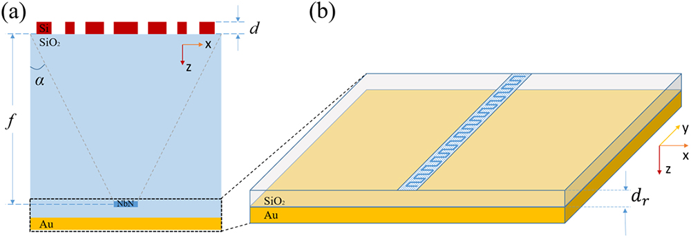
    Fig. 1. (a) Schematic diagram of the structure of HCG-SNSPD. HCG is located at the top of the structure. It is made of a high-refractive-index material Si with a thickness of d. There is a vacuum gap between the gratings. The material of the layer below HCG is SiO2. Incident light passes through HCG to focus on the SiO2 layer. The focal length is f. The NbN nanowire is located at the focal position, and there are several thick layers of SiO2 and an Au layer below the nanowires. α is the angle between the gray dotted line (from the edge of the structure to the focal point) and the vertical direction. (b) Schematic diagram of the position of the nanowires, resonant cavity, and Au mirror at the bottom of the HCG-SNSPD. The shaded part indicates the focused bar, the meandering structures are the nanowires, and dr is the thickness of the resonant cavity.
    (a) Schematic diagram of HCG design. The upper part is a 3D structural view of the grating. The TM-polarization plane wave is incident from the top, downwards toward the HCG. The lower part is the front view of the grating along the y-axis direction. pn and rn are the width and center position of each grating bar, respectively, and ϕ(rn) is the phase shift that should be satisfied when focusing. The position of r0 is defined as the origin of the x axis. (b) Comparison of the phase shifts corresponding to the grating parameters selected for the design with the ideal phase shift curve. The discrete red dots are the selected phase, and the solid black line is the ideal phase, corresponding to the left and lower axes. The value of x corresponding to each red dot represents the position of each grating bar rn on the x axis. The blue square line is the design focal length versus transmittance, corresponding to the right and upper axes. (c) Transmittance table and (d) phase shift table of incident light passing through the HCG with thickness d=0.75 μm. Areas with transmittance greater than 90% are surrounded by the solid line in both figures. Considering processing difficulty, aspect ratios of the parameters in the lower-left corner are too small to be included as candidates, and they are shown as zero value.
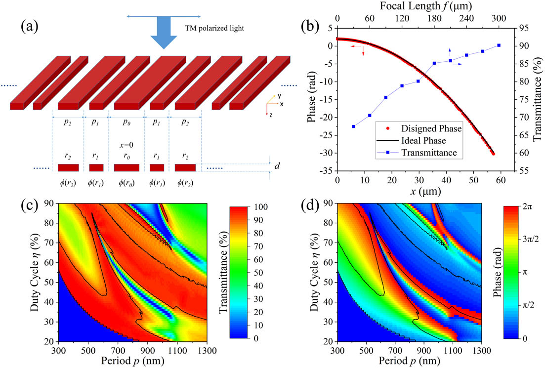
    Fig. 2. (a) Schematic diagram of HCG design. The upper part is a 3D structural view of the grating. The TM-polarization plane wave is incident from the top, downwards toward the HCG. The lower part is the front view of the grating along the y-axis direction. pn and rn are the width and center position of each grating bar, respectively, and ϕ(rn) is the phase shift that should be satisfied when focusing. The position of r0 is defined as the origin of the x axis. (b) Comparison of the phase shifts corresponding to the grating parameters selected for the design with the ideal phase shift curve. The discrete red dots are the selected phase, and the solid black line is the ideal phase, corresponding to the left and lower axes. The value of x corresponding to each red dot represents the position of each grating bar rn on the x axis. The blue square line is the design focal length versus transmittance, corresponding to the right and upper axes. (c) Transmittance table and (d) phase shift table of incident light passing through the HCG with thickness d=0.75  μm. Areas with transmittance greater than 90% are surrounded by the solid line in both figures. Considering processing difficulty, aspect ratios of the parameters in the lower-left corner are too small to be included as candidates, and they are shown as zero value.
    Simulation results of the designed HCG with f=300 μm. (a) Normalized energy field distribution of the cross section of the HCG. The actual focal point appears at 296 μm from the grating. (b) Normalized energy distribution curves along the line x=0 (red curve). (c) Normalized energy distribution curves along the line z=296 μm (blue curve). The inset shows a magnified view of the −5 μm<x<5 μm region with an FWHM of 2.5 μm.
    Fig. 3. Simulation results of the designed HCG with f=300  μm. (a) Normalized energy field distribution of the cross section of the HCG. The actual focal point appears at 296 μm from the grating. (b) Normalized energy distribution curves along the line x=0 (red curve). (c) Normalized energy distribution curves along the line z=296  μm (blue curve). The inset shows a magnified view of the 5  μm<x<5  μm region with an FWHM of 2.5 μm.
    (a) Transmittance spectrum at the focal plane. The red, blue, and green solid lines indicate the transmittance across the focal plane, the central 30-μm width, and the central 10-μm width, respectively. (b) Absorption of nanowire as a function of θ of the incident light from 1450 nm to 1650 nm. The inset shows a schematic of the simulated structure, and θ is defined as the angle between the incident direction and the vertical direction.
    Fig. 4. (a) Transmittance spectrum at the focal plane. The red, blue, and green solid lines indicate the transmittance across the focal plane, the central 30-μm width, and the central 10-μm width, respectively. (b) Absorption of nanowire as a function of θ of the incident light from 1450 nm to 1650 nm. The inset shows a schematic of the simulated structure, and θ is defined as the angle between the incident direction and the vertical direction.
    (a) Absorption spectrum of HCG-SNSPD. The red squares and blue dots indicate the absorption with and without cavity structure, respectively. The inset shows the normalized energy field distribution results for the nanowire integrated with the cavity at the wavelength of 1550 nm. The widths of the field area in the horizontal and vertical directions are 18 μm and 4 μm, respectively. The nanowires are located in the dotted rectangle. (b) Absorption efficiency as a function of resonant cavity thickness (130 nm<dr<380 nm, the region in the dotted box in the inset). The inset shows the absorption curve at a wider variety of thickness (50 nm<dr<2170 nm).
    Fig. 5. (a) Absorption spectrum of HCG-SNSPD. The red squares and blue dots indicate the absorption with and without cavity structure, respectively. The inset shows the normalized energy field distribution results for the nanowire integrated with the cavity at the wavelength of 1550 nm. The widths of the field area in the horizontal and vertical directions are 18 μm and 4 μm, respectively. The nanowires are located in the dotted rectangle. (b) Absorption efficiency as a function of resonant cavity thickness (130  nm<dr<380  nm, the region in the dotted box in the inset). The inset shows the absorption curve at a wider variety of thickness (50  nm<dr<2170  nm).
    Absorption efficiency as a function of the filling factor. The red squares and blue triangles indicate the absorption of nanowires with 8-nm and 6-nm thickness, with different filling factors, respectively. The inset shows a schematic diagram of the filling factor.
    Fig. 6. Absorption efficiency as a function of the filling factor. The red squares and blue triangles indicate the absorption of nanowires with 8-nm and 6-nm thickness, with different filling factors, respectively. The inset shows a schematic diagram of the filling factor.
    Influence of fabrication tolerances on absorption results (at the wavelength of 1550 nm). (a) Absorption as a function of the thickness d and the ratio of bar width wg of the grating. The inset illustrates the grating parameters represented by d and wg in the structure. (b) Absorption as a function of vertical and horizontal deviations of nanowire positions. The inset shows the vertical and horizontal deviation positions of the nanowires. Due to the symmetry, the horizontal deviation is shown in one direction. The positive and negative values of the vertical deviation represent the downward and upward shifts, respectively.
    Fig. 7. Influence of fabrication tolerances on absorption results (at the wavelength of 1550 nm). (a) Absorption as a function of the thickness d and the ratio of bar width wg of the grating. The inset illustrates the grating parameters represented by d and wg in the structure. (b) Absorption as a function of vertical and horizontal deviations of nanowire positions. The inset shows the vertical and horizontal deviation positions of the nanowires. Due to the symmetry, the horizontal deviation is shown in one direction. The positive and negative values of the vertical deviation represent the downward and upward shifts, respectively.
    Chen Wei, Wencong Wang, Dongmei Liu, Min Gu, Xianqiu Wu. High-efficiency and large light-receiving area superconducting nanowire single-photon detector integrated with high-contrast grating[J]. Photonics Research, 2021, 9(11): 2253
    Download Citation